| Posted: August 4, 2010 |
Researchers develop 120nm III-V high-electron-mobility transistors with cut-offs above 100 GHz |
| (Nanowerk News) Researchers based in China have developed 120nm III-V high-electron-mobility transistors (HEMTs) with millimeter-wave broadband and satellite communication applications in mind [Huang Jie et al, J. Semicond., vol31, p074008, 2010]. The current-gain cut-off frequency (fT) was 141GHz and the maximum power gain cut-off was (fmax) 120GHz. |
| The research was carried out by scientists from Chinese Academy of Sciences' Institute of Microelectronics and China's Southwest University in Chongqing. The researchers see their new indium gallium arsenide/indium aluminum arsenide (InGaAs/InAlAs) devices as being "promising in millimeter-wave devices and integrated circuits". Table 1: InGaAs/InAlAs HEMT epitaxial layer structure. |
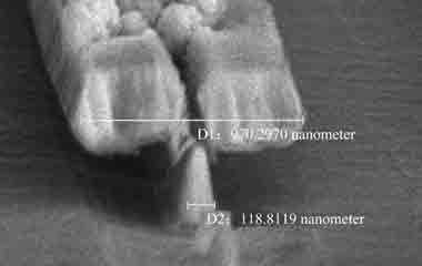 |
| SEM photo of T-shaped pattern of the InGaAs/InAlAs HEMT. |
| The device structures were grown on semi-insulating indium phosphide (InP) substrates using molecular beam epitaxy (MBE). To make the transistors, the source and drain regions were formed first using the deposition and lift-off of six layers of alloyed metal (nickel, germanium, gold, germanium, nickel, gold). The resulting contact resistance was measured at 0.2Ω-mm using the transmission line model (TLM). |
| The mesa isolation structures were formed by a wet chemical etch using an aqueous solution of phosphate (H3PO4) and hydrogen peroxide. Electron-beam evaporation was used to create the titanium-gold wiring. |
| To produce short gate lengths of ∼100nm, the researchers developed a four-layer electron-beam resist process – poly(methyl methacrylate) (PMMA), polymethylglutarimide (PMGI), ZEP520, polymethylglutarimide (PMGI). ZEP520 is a high-performance resist developed by Zeon Corp of Japan. The China researchers report that use of the bottom PMGI layer helps in the clean removal of the resist layers compared with a structure that has a ZEP520 bottom layer. |
| The gate (see Figure above) was recessed into the cap layer with a wet citric acid/hydrogen peroxide etch that was stopped by an InP etch-stop layer (selectivity InGaAs/InP ~160). The gate metal consisted of titanium, platinum and gold, which was deposited in an evaporation and lift-off process. A T-gate shape was used to reduce parasitic capacitance and resistance effects. The gate had a 120nm length and a 2x50µm width. Passivation was not used because the researchers wanted to avoid increasing the gate capacitance and thus impact the high-frequency performance. |
| In DC operation, the HEMT's saturation drain-to-source current was found to be 446mA/mm. The maximum extrinsic transconductance (Gm) of 520mS/mm was obtained under conditions where the gate-source voltage was –0.5V and the drain-source voltage was 1.5V. Subthreshold, the gate leakage – a little less than 0.1µA – is dominated by current from the drain. The pinch-off/threshold voltage is –1V (hence the transistor is 'on' at 0V). |
| The frequency performance was extracted from measurements made in the range 0.1–26.1GHz. The maximum power gain cut-off was determined from measurements made at a drain–source voltage of 1.5V and a gate–source voltage of –0.5V. Parasitic effects were de-embedded from the measurements. |
| Source: Chinese Academy of Sciences |

