| Posted: August 4, 2010 |
Unprecedented look at oxide interfaces reveals unexpected structures on atomic scale |
|
(Nanowerk News) Thin layers of oxide materials and their interfaces have been observed in atomic resolution during growth for the first time by researchers at the Center for Nanophase Materials Sciences at the Department of Energy's Oak Ridge National Laboratory, providing new insight into the complicated link between their structure and properties.
|
|
"Imagine you suddenly had the ability to see in color, or in 3-D," said the CNMS's Sergei Kalinin. "That is how close we have been able to look at these very small interfaces."
|
|
The paper was published online in ACS Nano with ORNL's Junsoo Shin as lead author.
|
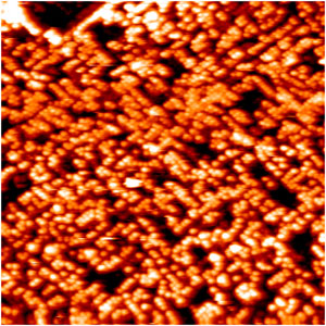 |
| A new scanning tunneling microscopy and low energy electron diffraction technique developed at Oak Ridge National Laboratory captured this 50 nm x 50 nm image of an oxide surface. Each bright dot is a single atom of material.
|
|
A component of magnetoelectronics and spintronics, oxide interfaces have the potential to replace silicon-based microelectronic devices and improve the power and memory retention of other electronic technologies.
|
|
However, oxide interfaces are difficult to analyze at the atomic scale because once the oxides are removed from their growth chamber they become contaminated. To circumvent this problem, ORNL researchers led by Art Baddorf built a unique system that allows scanning tunneling microscopy and low energy electron diffraction to capture images of the top layer of the oxide while in situ, or still in the vacuum chamber where the materials were grown by powerful laser pulses.
|
|
Many studies of similar oxide interfaces utilize a look from the side, typically achieved by aberration corrected scanning transmission electron microscopy (STEM). The ORNL team has used these cross-sectional images to map the oxide organization.
|
|
However, like a sandwich, oxide interfaces may be more than what they appear from the side. In order to observe the interactive layer of the top and bottom oxide, the group has used scanning tunneling microscopy to get an atomically resolved view of the surface of the oxide, and observed its evolution during the growth of a second oxide film on top.
|
|
"Instead of seeing a perfectly flat, square lattice that scientists thought these interfaces were before, we found a different and very complicated atomic ordering," said Baddorf. "We really need to reassess what we know about these materials."
|
|
Oxides can be used in different combinations to produce unique results. For instance, isolated, two oxides may be insulators but together the interface may become conductive. By viewing the atomic structure of one oxide, scientists can more effectively couple oxides to perform optimally in advanced technological applications such as transistors.
|
|
Kalinin says the correct application of these interface-based materials may open new pathways for development of computer processors and energy storage and conversion devices, as well as understanding basic physics controlling these materials.
|
|
"In the last 10 years, there has been only limited progress in developing beyond-silicon information technologies," Kalinin said. "Silicon has limitations that have been reached, and this has motivated people to explore other options."
|
|
Atomic resolution of interface structures during oxide growth will better enable scientists to identify defects of certain popular oxide combinations and could help narrow selections of oxides to spur new or more efficient commercial applications.
|

