| Posted: August 19, 2010 |
Understanding gate oxide trapping - one electron at a time |
| (Nanowerk News) Using a new technique, researchers from imec, TU Vienna, and Infineon have shown that both electron and hole capture and emission times in SiO2 and HfO2 dielectrics are strongly thermally activated. The new technique, Time Dependent Defect Spectroscopy (TDDS), can be used to study the capture and emission times of single oxide defects over a very wide time range. This knowledge will help to better understand the time variability of future deeply scaled devices, as well as the operation of charge-storage memories. |
| Negative Bias Temperature Instability (NBTI) is a critical reliability issue in modern CMOS technologies. Despite several decades of research, there is still no consensus about the exact mechanisms involved in NBTI. In 2009, researchers from imec and TU Vienna have argued that the phenomenon called NBTI relaxation in pFET devices is another facet of the well-known low-frequency noise in these devices. While the low-frequency noise corresponds to the channel/gate dielectrics system being in the state of dynamic equilibrium, NBTI relaxation corresponds to the perturbed system returning to this equilibrium. This finding could signify a fundamental advance in the understanding of NBTI. |
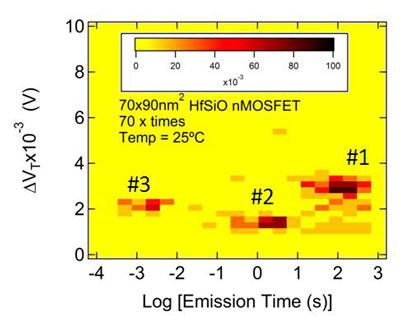 |
| Gate oxide trapping.jpg: TDDS spectrum taken on a 70x90nm2 nMOSFET with 1nm SiO2 and 1.8nm HfSiO gate oxide showing 3 distinct defects. |
| Continued research has now yielded new insights into the trapping phenomena in gate oxides in deeply scaled FETs. In such devices, the relaxation is observed to proceed in discrete voltage steps, with each step corresponding to the discharge of a single oxide defect. Upon repeated perturbation, each defect shows up in the relaxation trace with a characteristic fingerprint consisting of its discharge, or emission time, and its voltage step. It is possible to construct a spectrum mapping the properties of up to a dozen of individual defects. The capture time of each defect is obtained by varying the perturbation time. Contrary to techniques for the analysis of random telegraph noise (RTN), which only allow monitoring the defect behavior in a rather narrow time window, the new TDDS technique can be used to study the capture and emission times of the defects over an extremely wide time range. |
| Using this new technique, researchers from imec, TU Vienna, and Infineon have shown that both electron and hole capture and emission times in SiO2 and HfO2 dielectrics are strongly thermally activated. Such behavior is incompatible with elastic tunneling, but is consistent with the non-radiative multiphonon theory previously applied to the analysis of RTN. A quantitative model based on this theory explains the bias as well as the temperature dependence of the characteristic time constants. Apart from the reliability issues, the model is also applicable to charge-storage memories. |
| The knowledge generated from the research is moreover directly useful for understanding time variability of future deeply scaled devices. Imec researchers observe that in 70 x 90nm2 pFETs, a single-carrier discharge event can cause a voltage shift exceeding 30mV, which is the failure criterion typically used to determine the device lifetime. The overall device-to-device threshold voltage shift distribution after NBTI stress is argued to be a convolution of exponential voltage distributions of uncorrelated individual charged defects Poisson-distributed in number. An analytical description then allows, among other things, to calculate NBTI threshold voltage shifts in an unlimited population of devices, a feat impossible through device simulations. These findings, presented at the 2010 International Reliability Physics Symposium, shed new light on our understanding of NBTI and can lead to a more accurate prediction of the NBTI lifetime. |
| Source: imec |

