| Nov 24, 2010 |
Plasmonics: Smooth operator |
| (Nanowerk News) Surface plasmon resonance—the coherent excitation of free electrons on the surface of metals—is crucial to the operation of extremely small photonic devices, which have applications ranging from optoelectronic circuits and molecular sensors to the 'metamaterials' that could one day be used to make invisibility cloaks. To minimize scattering losses in metals, the metal surfaces need to be extremely smooth. Jinghua Teng at the A*STAR Institute of Materials Research and Engineering and co-workers have now developed an effective method to fabricate smooth thin films of silver with enhanced plasmonic properties ("Enhanced Surface Plasmon Resonance on a Smooth Silver Film with a Seed Growth Layer"). |
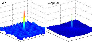 |
| Fig 1: Correlation plots showing the smoothness of thin silver films prepared on bare silicon (left) and on a germanium seed layer (right). The narrower and shorter the center peak, the smoother the film. |
| As surface plasmon resonances are confined to surfaces, it is possible to miniaturize plasmonic devices to sizes that go far below the wavelength of light used to excite the electrons, but at such dimenions, losses become an obstacle to performance. "One of the grand challenges for plasmonics and metamaterials application is the minimization of loss," says Teng. "Applications of plasmonics in real-world devices will to a great extent depend on our ability to fabricate structures with low optical losses." |
| These losses originate from absorption as well as the scattering of light due to small imperfections and roughness on the surface of a metal. Therefore, it is paramount to use metal films with ultrasmooth surfaces. At the same time, the fabrication technique used for preparing the metal films needs to be scalable for industrial applications—and evaporative deposition techniques are currently the best option. |
| The researchers have now optimized the evaporation technique for depositing thin silver films on silicon and quartz substrates. They first deposited a seed layer of nickel or germanium on the substrate, then deposited the silver. The seed layer leads to a smoother surface, and the researchers found the silver–germanium film to be the smoothest (Fig. 1). However, because of optical losses in germanium, the silver–nickel films showed superior plasmonic properties. "Overall, the silver–nickel structure is the best because of its low losses and enhanced plasmonic properties," says Teng, "It will be an essential material for future low-loss plasmonic device applications." |
| The researchers are now searching for ways to enhance the plasmonic and metamaterial devices. "We are now trying to apply this silver–nickel film in applications like superlenses to achieve higher resolution in optical imaging. It can also be implemented in many other plasmonic devices and applications, such as metamaterials and plasmonic circuits," says Teng. |
| Source: A*STAR |

