| Dec 02, 2010 |
Direct writing of sub-5 nm metallic nanostructures |
| (Nanowerk News) A group of Beckman Institute researchers have discovered a practical method for direct writing of metal lines less than five nanometers (5 nm) wide, a big step in creating contacts to and interconnects between nanoscale device structures like carbon nanotubes and graphene that have potential uses in electronics applications. |
| The research was led by Beckman faculty members Joe Lyding, Gregory Girolami and Angus Rockett, with Lyding student Wei Ye as lead author. Their paper reporting the research is titled Direct Writing of Sub-5 nm Hafnium Diboride Metallic Nanostructures and appeared in the journal ACS Nano ("Direct Writing of Sub-5 nm Hafnium Diboride Metallic Nanostructures"). |
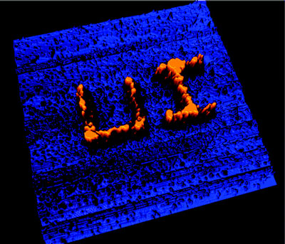 |
| Sub-5 nm metallic hafnium diboride (HfB2) nanostructures were directly written onto Si(100)-2 × 1:H surfaces using ultrahigh vacuum scanning tunneling microscope (UHV-STM) electron beam induced deposition (EBID) of a carbon-free precursor molecule, tetrakis(tetrahydroborato)hafnium. |
| Recent research by Lyding's group has demonstrated methods for depositing graphene on semiconducting substrates and creating semiconducting carbon nanotubes that make these carbon-based materials practical candidates for integration into electronics and other devices that now rely on silicon and metals to operate. In this paper, the researchers report on a technique for the patterning of metallic nanostructures on surfaces toward future fabrication of nanoelectronics and quantum devices. |
| The researchers write that "Current top-down fabrication technologies used in industry involve conventional lithographic processes, which are approaching their fundamental size limits. Responding to the current challenges involving fabrication at scales smaller than 10 nm, they have demonstrated "the ability to write metal lines that are less than 5nm wide. |
| "To do this we use the electrons from our STM tip to 'crack' molecules that are introduced in the gas phase to the STM tip-sample junction. The procedure of using STM electrons to break apart molecules and yield a metallic deposit is not new, however previous attempts have been plagued by high levels of carbon impurities in the deposits and metallic behavior had not been demonstrated. To circumvent this issue we used a novel molecular precursor for the metallic ceramic hafnium diboride that was developed by Prof. Gregory Girolami's group for low temperature chemical vapor deposition (CVD) applications." |
| They add that "Girolami's CVD precursor contains no carbon; only hafnium, boron and hydrogen. Electron beam induced deposition (EBID) by the STM cleanly drives out the hydrogen leaving a metallic HfB2 deposit, as confirmed by STM spectroscopy." |
| They conclude by writing that "To our knowledge this is the first demonstration of sub-5 nm metallic nanostructures in an STM-EBID experiment, and it opens new opportunities for making deterministic molecular scale metallic contacts." |
| Source: University of Illinois at Urbana-Champaign |

