| Dec 08, 2010 |
Photonics: The full spectrum |
| (Nanowerk News) White light-emitting diodes (LEDs) are increasingly finding applications from indoor lighting to flat panel displays. Their success is founded on advances in the growth of semiconductor compounds based on nitrogen, in particularly the blue light emitters aluminum nitride (AlN) and gallium nitride (GaN), which are the key compounds used in white LEDs. Another nitride semiconductor, indium nitride (InN) is also of interest for its red and infrared light emission. Together, all three compounds could cover the entire visible spectrum, from red to violet. |
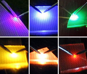 Examples of LEDs based on various semiconductor compounds. Unfortunately, however, the growth of InN thin films with sufficient quality has been difficult. Wei Liu at A*STAR's Institute of Materials Research and Engineering and co-workers have now developed a growth technique and layer design that overcomes previous fabrication problems with InN LEDs ("The effects of cap layers on electrical properties of indium nitride films"). One of the problems in growing high-quality InN thin films is the development of electrical charge on the surface of samples during growth. All LEDs contain a p–n junction comprising two neighboring regions—one with a surplus of negative charge and one with a surplus of positive charge. The surface charge compensates for charge at the p–n junction, and also leads to defects that slow down the electrons as they move through the InN film. Both effects are detrimental to the operation of LEDs. The researchers have now discovered a solution to this problem. "We have demonstrated that a cap layer is able to overcome this problem," says Liu. The problem with charge accumulation is limited to InN, so a very thin cap layer made from another nitride semiconductor such as SiN, GaN or ZnN is sufficient to prevent the development of surplus electrical charge. |
| The impact of the cap layer on the sample quality is significant. An example is the transport of electrons. With the cap layer, the electrons move more than 100 times faster through the InN, promising significant performance enhancements for LEDs and other electronic devices. |
| The realization of efficient InN LEDs will make it possible to achieve complete coverage of the visible spectrum using nitride-based semiconductors. "This means that group-III nitrides can completely replace gallium arsenide and indium phosphide as materials for yellow, red and infrared LEDs," says Liu. The advantage is that LEDs of all colors can be grown on the same chip in a single growth process. In addition, according to Liu this has considerable environmental benefits. "Gallium arsenide and indium phosphide are toxic materials and the precursors used for their growth are also toxic. GaN, AlN and InN, on the other hand, are environmentally friendly materials." |
| Source: A*STAR |

