| Dec 14, 2010 |
Making wafers faster by making features smaller |
| (Nanowerk News) The manufacturing of semiconductor wafers used in all types of electronics involves etching small features onto a wafer with lasers, a process that is ultimately limited by the wavelength of the light itself. The semiconductor industry is rapidly approaching this fundamental limit for increasing the speed of the microchip. The development of a new intense 13.5-nm (extreme ultraviolet or EUV) light source will resolve this issue by reducing the feature size by an order of magnitude or so, according to Purdue researchers in the Journal of Applied Physics ("Analysis of atomic and ion debris features of laser-produced Sn and Li plasmas"). |
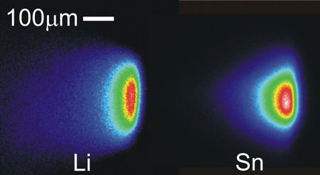 |
| False-color images of the tin and lithium plasma plumes in EUV emission through a 7 to 15 nm filter, obtained under identical conditions. |
| One way to generate this wavelength of light is to bombard tin (Sn) and lithium (Li) targets with laser beams to create an intensely bright plasma; Sn and Li are good candidates because their plasmas emit efficiently in the 13.5 nm region, says Purdue graduate student Ryan Coons. He and his colleagues used spectroscopy and a Faraday cup to analyze the emission features and debris produced in laser-produced tin and lithium plasmas, and others in his group modeled their physical processes. |
| In a detailed comparison of the atomic and ionic debris, as well as the emission features of Sn and Li plasmas, the group's results show that Sn plasmas produce twice as much emission as that of Li. However, the kinetic energy of Sn ions is considerably higher, though with a lower flux. More work is needed to perfect the development of this technology. |
| Source: American Institute of Physics (AIP) |

