| Dec 18, 2010 |
Study to avoid stress impact of 3D stacking on IC performance |
| (Nanowerk News) At IEDM 2010, imec and its partners presented a study of the stress-induced impact of through-silicon via (TSV) processing on the performance of high-k/metal-gate CMOS transistors and circuits. This study is a first of its kind; the results and the approach that was followed are a foundation for stress-aware design with dedicated design rules. This will allow to precisely delineate keep-out zones (KOZ), and thus to save valuable silicon area. |
| In 3D stacking, one of the concerns is the potential impact of TSVs and TSV processing on the integrity of the transistors and circuits. This impact will depend on the mechanical stress in the final stack, but also on the stresses that the silicon undergoes during TSV processing. Most challenging is the heating during TSV processing, which will cause a mechanical stress in the silicon surrounding the TSVs because of the mismatch in thermal expansion coefficient between the Cu TSV and the silicon. |
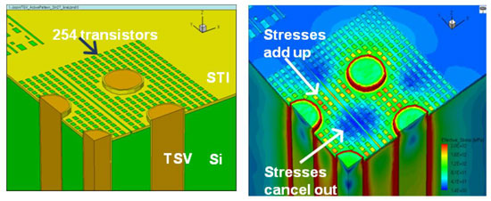 |
| Left) Simulated test structure reproducing measurements on a transistor array. (Right) Stress distribution around the TSV matrix showing that in certain regions the stress can be amplified or cancelled out. |
| This stress negatively affects the carrier mobility and the performance of the transistors located near to the TSVs. To mitigate these negative effects, and using standard design rules, large layout areas will have to be sacrificed. The alternative is to use dedicated design rules, which take into account the exact stress locations. In this study, the mechanical stress and its impact are examined in detail, for a variety of TSV placement patterns and transistor sizes, with the aim to have a foundation to derive robust, dedicated design rules that can save valuable silicon area. |
| The method used is a combination of theoretical modeling and experimental measurements. For the modeling, a finite element model (FEM) was set up based on, a.o. measured TSV Cu properties and process temperature profiles. For the experimental measurements, test structures with various TSV alignments were processed on imec's 300mm 3D-SIC via-first baseline process. Both analog test structures (consisting of 12-bit DAC circuits) and digital test structures (using 40nm FETs) were used. The results obtained through modeling closely matched those from the experimental setup. |
| The results of the study show, both for the analog and digital test structures, and for various TSV layouts, the dimensions of the KOZ. For a digital FET, the KOZ will grow from 6µm to 20µm with a growing number of TSVs in the array. In general, the results show that short-channel transistors such as 40nm MOSFETs will exhibit an Idsat variation around 9% nearby TSVs. The resulting KOZ for a matrix of TSVs will measure 200µm for analog circuits and 20µm for digital circuits. The study shows that there is a complex interaction of stresses. The dedicated design rules that can be derived will precisely delineate the keep-out-zones, saving valuable silicon area. |
| Source: imec |

