| Dec 24, 2010 |
Researchers fabricate first single crystal diamond nanoelectromechanical switch
|
|
(Nanowerk News) Dr. Meiyong Liao, a Senior Researcher of Sensor Materials Center, National Institute for Materials Science (NIMS), cooperated with his colleagues, succeeded in the batch fabrication of suspended structures (cantilevers and bridges) of single crystal diamond for nano/micro electromechanical system (NEMS/MEMS). Based on this process, they achieved in the world the first single crystal diamond NEMS switch.
|
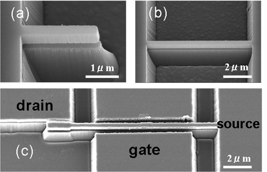 |
| Scanning electron microscope images of the suspended structures of single crystal diamond, (a) cantilever, (b) bridge, and (c) 3-terminal NEMS switch. Air gap structure has been formed in the substrate side.
|
|
The NEMS switch has the advantages of low-leakage current, low-power consumption and sharp on/off ratio in comparison with the conventional semiconductor devices. Most of the existing NEMS/MEMS switches are based silicon or metal materials, which, however, have the drawbacks of poor mechanical, chemical, and thermal stability, poor reliability and durability. Diamond is the ideal material for NEMS/MEMS due to the highest elastic modulus, mechanical hardness, thermal conductivity, and variable electrical conductivity from insulator to conductor. However, due to the difficultly in fabricating suspended structures of single crystal diamond, the development of single crystal diamond NEMS/MEMS devices has been a challenge.
|
|
The NIMS research team developed a process for fabricating suspended single crystal diamond structures by locally forming a graphite sacrificial layer in a single crystal diamond substrate by high energy ion implantation, followed by the growth of a diamond epilayer with electrical conductivity by microwave plasma chemical vapor deposition method (MPCVD) and the removal of the graphite sacrificial layer. As a further development of this technique, the group also succeeded for the first time in fabricating NEMS switching devices with a transistor-like structure comprising 3 electrodes.
|
|
The leakage current of the developed diamond NEMS switch is very low, and the power consumption is less than 10pW (picowatt). The devices exhibit high reproducibility, high reliability and no surface stiction. Stable operation of the diamond NEMS switch in a high temperature environment (250°C) was also confirmed. The Young's modulus of the moveable cantilever structure was measured to be 1100GPa, which is close to the value of bulk diamond single crystals. Thus, high-speed (gigahertz) switching operation can be expected.
|
|
In comparison with the existing MEMS switches, the diamond NEMS switches are expected to show greatly improved functions, including reliability, lifetime, speed, and electrical handling capacity, etc. The developed devices can be applied as microwave switch for next-generation wireless communications and logic circuit under harsh environments. These research results also establish the infrastructure for diamond NEMS/MEMS with novel functions, opening the way for the development of various chemical, physical, and mechanical sensors.
|

