| Jan 28, 2011 |
Development of a 0.5 nm ultra-thin high-permittivity gate insulating film
|
|
(Nanowerk News) Hiroyuki Ota and Shinji Migita, the Nanostructured CMOS Research Team, the Nanodevice Innovation Research Center of the National Institute of Advanced Industrial Science and Technology (AIST), have developed a new technology for the production of 0.5 nm ultra-thin high-permittivity gate insulating films.
|
|
This technology uses improved existing manufacturing processes for semiconductor devices. By focusing on the crystallization process of a high-permittivity material and incorporating a heat treatment that enables precise control of crystal growth, the researchers have developed the technology for the synthesis of high-permittivity crystalline films with no low-permittivity layer at the boundary with the substrate. When employed as MOS transistor gate insulating films, the high-permittivity crystalline films synthesized using this technology can achieve an equivalent silicon oxide (SiO2) thickness of 0.5 nm, and have been shown to reduce leakage current by six orders of magnitude. Since leakage current from MOS transistor gate insulating films accounts for a significant proportion of the power consumption of integrated circuits, the new high-permittivity gate insulating film is expected to contribute to the manufacture of integrated circuits with lower power consumption.
|
|
This research and development was commissioned by "Next-generation Semiconductor Materials and Process Technology (MIRAI) Project" of the New Energy and Industrial Technology Development Organization (NEDO). The details of the technology were presented at the International Electron Devices Meeting, held in San Francisco from December 6 to 8, 2010.
|
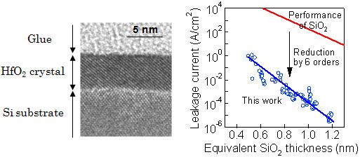 |
| Figure 1: Electron micrograph of high-permittivity crystalline film (HfO2) grown directly on silicon substrate (left); Reduction in leakage current (right)
|
|
Social Background of Research
|
|
Today, with the widespread use of cell phones, personal computers, high-performance televisions, and other devices, power consumption by electronic devices is increasing across society as a whole. The reduction of this power consumption is an important technological issue that will contribute to the reduction of CO2 emissions. Integrated circuits, the central elements in electronic devices, are each composed of several hundred million MOS transistors, and the reduction of leakage current from the gate insulating films of each of these transistors will assist in reducing power consumption in electronic devices as a whole.
|
|
Semiconductor manufacturers, universities, and research institutes throughout the world have been engaged in research and development of transistor gate insulating films using high-permittivity materials in order to reduce the leakage current from the films. At present, gate insulating films with an equivalent silicon oxide thickness of 1 nm have been developed, and integrated circuits using this technology are in manufacture. The semiconductor industry has stated that, from 2013 thicknesses of 0.65 nm will be necessary, and in 2015 this figure will be 0.53 nm. Research and development are being conducted throughout the world to realize these targets.
|
|
History of Research
|
|
AIST has conducted research and development of high-permittivity gate insulating films, including the development of a technology to reduce impurities through the combination of an atomic layer growth technology and a rapid heat treatment technology, and the elucidation of the effect of the dipoles generated at the boundary between high-permittivity materials and silicon oxide films on the threshold voltage for transistor operation and the reduction of mobility. AIST has world-leading potential in this field.
|
|
The present study was commissioned by the NEDO project, "Next-generation Semiconductor Materials and Process Technology (MIRAI) Project". This collaborative project among government, academia, and private enterprises is seeking to develop next-generation semiconductor materials and fundamental process technologies, and numbers AIST, universities, and device and equipment manufacturers among its participants.
|
|
Details of Research
|
|
The new technology was developed on the basis of the proposal of a new method of synthesizing crystalline films of a high-permittivity material. Up to the present, companies and research institutes throughout the world have made numerous attempts to produce high-permittivity gate insulating films using crystalline films. Using special film formation techniques for research applications, the superiority of crystalline films has been demonstrated. However, when high-permittivity crystalline films are synthesized by means of industrial-use manufacturing processes, the thickness of the film increases and leakage current rises due to the formation of a low-permittivity layer, and because of this it is extremely difficult to manufacture insulating films displaying a level of performance appropriate for practical use. The present development therefore attempted to overcome this previously unresolved problem by modifying the process of crystallization while employing industrial-use equipment.
|
|
Figure 1 (right) shows the relationship between the equivalent silicon oxide thickness and the leakage current measured with a gate electrode formed on the HfO2 crystal film synthesized on the silicon substrate. The newly developed technology has reduced leakage current by six orders of magnitude against silicon oxide films. At its thinnest, 0.5 nm, the film displays a leakage current of only 1 A/cm2. We believe that if this newly developed technology enters practical use, targets for the development of gate insulating films for the next ten years can be met.
|
|
Figure 2 shows a model of the developed processes. First, an amorphous HfO2 film is deposited on a silicon substrate by means of atomic layer deposition. Next, a high-temperature heat treatment is applied to crystallize the amorphous film. At this time, heat transfer from the silicon substrate is used to let crystallization commence from the boundary with the substrate. This makes it possible to prevent the growth of a low-permittivity layer at the boundary. In addition, the uniform direction of crystal growth ensures that a dense crystalline film without voids is obtained, enabling increases in leakage current to be suppressed.
|
|
The developed technology can be realized using similar materials and equipment to those employed on existing semiconductor device production lines, and we believe that there will be few impediments to its practical use.
|
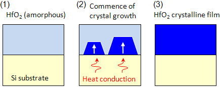 |
| Figure 2: Synthesis of the developed high-permittivity crystalline film (HfO2). (1) Deposition of amorphous HfO2 film on silicon substrate; (2) Heat transfer from the substrate promotes crystal growth from the boundary with the substrate; (3) Completion of formation of dense crystalline film without voids.
|
|
Future Plans
|
|
We intend to test the process-tolerance, variability in electrical characteristics, and reliability of the developed structure more systematically, in order to contribute to the future development of lower power consumption devices.
|

