| Jan 30, 2011 |
A new transistor: Thinner than silicon and better than graphene
|
|
(Nanowerk News) Smaller and more energy-efficient electronic chips could be made using molybdenite. In an article appearing online January 30 in the journal Nature Nanotechnology ("Single-layer MoS2 transistors"), EPFL's Laboratory of Nanoscale Electronics and Structures (LANES) publishes a study showing that this material has distinct advantages over traditional silicon or graphene for use in electronics applications.
|
|
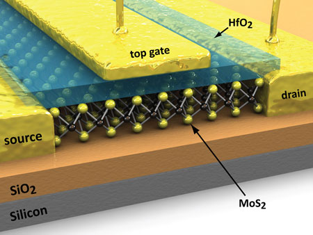
A discovery made at EPFL could play an important role in electronics, allowing us to make transistors that are smaller and more energy efficient. Research carried out in the Laboratory of Nanoscale Electronics and Structures (LANES) has revealed that molybdenite, or MoS2, is a very effective semiconductor. This mineral, which is abundant in nature, is often used as an element in steel alloys or as an additive in lubricants. But it had not yet been extensively studied for use in electronics.
|
 |
| Molybdenite is a two-dimensional material, very thin and easy to use in nanotechnology. It has real potential in the fabrication of very small transistors, light-emitting diodes (LEDs) and solar cells.
|
|
100,000 times less energy
|
|
"It's a two-dimensional material, very thin and easy to use in nanotechnology. It has real potential in the fabrication of very small transistors, light-emitting diodes (LEDs) and solar cells," says EPFL Professor Andras Kis, whose LANES colleagues M. Radisavljevic, Prof. Radenovic et M. Brivio worked with him on the study. He compares its advantages with two other materials: silicon, currently the primary component used in electronic and computer chips, and graphene, whose discovery in 2004 earned University of Manchester physicists André Geim and Konstantin Novoselov the 2010 Nobel Prize in Physics.
|
|
One of molybdenite's advantages is that it is less voluminous that silicon, which is a three-dimensional material. "In a 0.65-nanometer-thick sheet of MoS2, the electrons can move around as easily as in a 2-nanometer-thick sheet of silicon," explains Kis. "But it's not currently possible to fabricate a sheet of silicon as thin as a monolayer sheet of MoS2." Another advantage of molybdenite is that it can be used to make transistors that consume 100,000 times less energy in standby state than traditional silicon transistors. A semi-conductor with a "gap" must be used to turn a transistor on and off, and molybdenite's 1.8 electron-volt gap is ideal for this purpose.
|
|
Better than graphene
|
|
In solid-state physics, band theory is a way of representing the energy of electrons in a given material. In semi-conductors, electron-free spaces exist between these bands, the so-called "band gaps." If the gap is not too small or too large, certain electrons can hop across the gap. It thus offers a greater level of control over the electrical behavior of the material, which can be turned on and off easily.
|
|
The existence of this gap in molybdenite also gives it an advantage over graphene. Considered today by many scientists as the electronics material of the future, the "semi-metal" graphene doesn't have a gap, and it is very difficult to artificially reproduce one in the material.
|

