| Feb 01, 2011 |
EU-funded team puts new semi-conductor material to the test
|
|
(Nanowerk News) The electronic chips of the future might not be made of silicon or even graphene but of a material called molybdenite (MoS2). EU-funded research presented in the journal Nature Nanotechnology demonstrates that molybdenite is a highly effective semi-conductor that could be used to make transistors both smaller and more energy efficient.
|
|
EU support for the work came from the 5-year FLATRONICS ('Electronic devices based on nanolayers') project, a EUR 1.8 million European Research Council (ERC) Starting Grant awarded to Professor Andras Kis of the Laboratory of Nanoscale Electronics and Structures (LANES) at the Ecole Polytechnique Fédérale de Lausanne (EPFL) in Switzerland in 2009. ERC grants are channelled through the Ideas Programme of the Seventh Framework Programme (FP7).
|
|
Molybdenite is a mineral readily available in nature. Currently its main uses are as an element in steel alloys and as an additive in lubricants. Until now, its potential as a semi-conductor has remained largely unexplored.
|
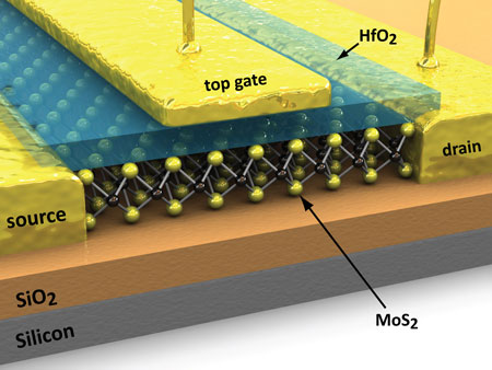 |
| Molybdenite is a two-dimensional material, very thin and easy to use in nanotechnology. It has real potential in the fabrication of very small transistors, light-emitting diodes (LEDs) and solar cells.
|
|
'It's a two-dimensional material, very thin and easy to use in nanotechnology,' says Professor Kis, who led the current study. 'It has real potential in the fabrication of very small transistors, light-emitting diodes (LEDs) and solar cells.'
|
|
According to Professor Kis and his colleagues, molybdenite offers significant advantages over silicon, which is widely used in electronics, and graphene, which is the most widely studied two-dimensional material and is commonly viewed as the electronics material of the future.
|
|
Silicon is a three-dimensional material, and so is more voluminous than molybdenite that can be fabricated in monolayers. 'In a 0.65-nanometre-thick sheet of MoS2, the electrons can move around as easily as in a 2-nanometre-thick sheet of silicon, but it's not currently possible to fabricate a sheet of silicon as thin as a monolayer sheet of MoS2,' explains Professor Kis.
|
|
Furthermore, transistors based on molybdenite would consume 100,000 times less energy in their standby state than conventional silicon transistors. This is because turning a transistor on and off requires a semi-conductor material with a 'band gap'. In physics, 'bands' are used as a way of describing the energy of electrons in a material. In semi-conductors, the term 'band gap' refers to the electron-free spaces between these bands. If the gap is neither too big nor too small, some electrons can jump across the gap, thereby offering researchers a way of controlling the electrical behaviour of the material and turning it on and off. Molybdenite has a 1.8 electron-volt band gap, making it ideal for turning transistors on and off.
|
|
Molybdenite's band gap also gives it the edge over graphene, which does not have a band gap in its pristine state. Although it is possible to make graphene that has a band gap, this increases the fabrication complexity and causes other problems.
|
|
'Our results provide an important step towards the realization of electronics and low-standby-power integrated circuits based on two-dimensional materials. Being a thin, transparent semiconducting material, MoS2 monolayers also present a wealth of new opportunities in areas that include mesoscopic physics, optoelectronics and energy harvesting,' the researchers conclude.
|
|
'With the possibility of fabricating large-area circuits using solution-based processing, our finding could be important for producing electronic devices that could combine the ease of processing associated with organic conductors with performance figures commonly associated with silicon-based electronics.'
|

