| Mar 04, 2011 |
Revolutionary SERS nanosubstrates for medical tests
|
|
(Nanowerk News) Laboratory on a microchip, capable to detect most types of antibodies in patient's blood in a single
test would be a revolutionary breakthrough in medical diagnostics. The physicians would gain rapid
access to examined patient's personal health records with the data on both past and present
diseases, as well as those that will develop only in future. This futuristic vision gets closer to reality
due to innovative, gold-coated gallium nitride substrates developed by researchers from the
Institute of Physical Chemistry of the Polish Academy of Sciences (IPC PAS) and the Institute of
High Pressure Physics of the PAS (IHPP PAS). Worldwide unique properties of the substrates
open for the first time the way to long expected dissemination of surface enhanced Raman
spectroscopy (SERS). Using this unusually sensitive research tool one can detect bacteria,
viruses, and even single molecules. "Lack of substrates with appropriate nanostructures has, for
last three decades, prevented SERS application in medicine. We managed finally to overcome the
obstacle" – says Prof. Robert Holyst (IPC PAS).
|
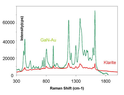 |
| SERS signal on gold-coated gallium nitride substrates developed by researchers from the Institute of Physical Chemistry of the Polish
Academy of Sciences (green) compared to commercially available substrates (red). (Source: IPC PAS)
|
|
Substrates with roughness features in nanometer scale play a key role in Raman spectroscopy.
The Raman effect is the inelastic scattering of photons on molecules. Usually a light scattering
molecule absorbs a photon and immediately emits another one with the same energy – the
phenomenon is termed by physicists elastic or Rayleigh scattering. Sometimes it happens,
however, that a part of photon energy is transferred, e.g., into vibrations or rotations of a molecule.
|
|
Then, the photon emitted by the molecule will have slightly lower energy. An opposite situation can
also happen: the molecule will give some energy to the emitted photon. In both cases the
scattering is known as Raman scattering, after the name of its discoverer, Indian physicist and
Nobel Prize winner Chandrasekhara Venkata Raman. The scattering is an extremely rare
phenomenon: only one photon per dozens of millions is scattered in that way, which means it is
very hard to detect.
|
|
In 1974, British chemist Martin Fleischmann with co-workers observed an unusually strong Raman
scattering signal from molecules placed on a roughened silver substrate. Further studies revealed
that the enhancement effect is real and occurs also on substrates made of gold, platinum and
copper. In each case, the necessary condition for enhancement to occur was an appropriate
surface morphology. "If the surface is appropriately roughened, the electromagnetic field intensity
on sharp edges of surface unevennesses is significantly increased. For a similar reason, all spire
structures attract thunderbolts" – explains Prof. Holyst. The molecules deposited on so prepared
surface are in a very strong electromagnetic field and much more frequently scatter photons
inelastically via Raman scattering. Surface Enhanced Raman Spectroscopy (SERS) is an
exceptionally attractive analytical tool yielding powerful enhancement of the original signal, usually
from million to billion times. So high method sensitivity allows detecting of even single molecules.
|
|
A good SERS substrate should have rather regular, periodic surface structure assuring that the
signals recorded by the measurement setup are reproducible. Its design is based on gallium nitride
(GaN) substrate, developed in the Institute of High Pressure Physics of the PAS. "The
manufacturing starts with fabrication of a GaN substrate covered evenly with structural defects of
nanometer size" – says D.Sc. Janusz Weyher from IHPP PAS. The surface is then photoetched,
the process takes place everywhere except for the defects and results in formation of vertical
pillars with approximately the same diameters. Due to tension forces, free terminals of adjacent
nanopillars attach to each other, forming numerous structures resembling stacks in the field. At that
stage, the substrates are transferred to the Institute of Physical Chemistry of the PAS, where a
thick gold layer is evaporated on to them. The process yields a surface coated with an even thicket
of nanometer size golden cones.
|
|
SERS substrates designed by Polish researchers have unique properties. "The substrates
commercially available so far had to be handled with extreme caution. They had to be stored under
nitrogen, could not be touched and even though they were loosing their enhancement ability within
hours only. Our substrates can be put into an ordinary drawer for a couple of months and they will
be still usable" – stresses Ph.D. Agnieszka Michota-Kaminska from the IPS PAS. For economic
reasons, it is important that Polish substrates are suitable for multiple use as the only ones
worldwide. Their surface structure is so stable that the researchers from the IPC PAS were able to
develop efficient cleaning procedures to assure that a high level of SERS signal enhancement is
maintained.
|
|
The substrates for SERS studies have been developed under the project "Quantum semiconductor
nanostructures for applications in biology and medicine". One of the project's long term goals is to
develop a sensor for detection of antibodies in blood. The core element of the device will be a
semiconductor with a surface network of thousands of micrometer size wells. Each well will contain
a specific carefully selected sequence of aminoacids to lure specific antibodies. A suitable
microfluidic system will provide blood, and the antibodies contained in blood will attach only to
matching polypeptides in wells. The data will be read out using SERS technique. The over 73
million PLN project is funded in 85% from the European Regional Development Fund under the
Innovative Economy Operational Programme 2007-2013. The main participants to the project are
the Institute of Physics of the PAS (coordinating body), the Institute of Physical Chemistry of the
PAS and the Institute of High Pressure Physics of the PAS.
|

