| Mar 28, 2011 |
Next-generation chemical mapping on the nanoscale
|
|
(Nanowerk News) A pixel is worth a thousand words? Not exactly how the saying goes, but in this case, it holds true: scientists at Berkeley Lab's Molecular Foundry have pioneered a new chemical mapping method that provides unprecedented insight into materials at the nanoscale ("Hyperspectral Nanoscale Imaging on Dielectric Substrates with Coaxial Optical Antenna Scan Probes").
|
|
Moving beyond traditional static imaging techniques, which provide a snapshot in time, these new maps will guide researchers in deciphering molecular chemistry and interactions at the nanoscale—critical for artificial photosynthesis, biofuels production and light-harvesting applications such as solar cells.
|
|
"This new technique allows us to capture very high-resolution images of nanomaterials with a huge amount of physical and chemical information at each pixel," says Alexander Weber-Bargioni, a postdoctoral scholar in the Imaging and Manipulation of Nanostructures Facility at the Foundry. "Usually when you take an image, you just get a picture of what this material looks like, but nothing more. With our method, we can now gain information about the functionality of a nanostructure with rich detail."
|
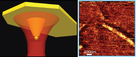 |
| Schematic of coaxial probe for imaging a carbon nanotube (left) and chemical map of carbon nanotube with chemical and topographical information at each pixel (right).
|
|
The Molecular Foundry is a U.S. Department of Energy (DOE) Office of Science nanoscience center and national user facility. With the Foundry's state-of-the-art focused ion beam tool at their disposal, Weber-Bargioni and his team designed and fabricated a coaxial antenna capable of focusing light at the nanoscale, – a harnessing of light akin to wielding a sharp knife in a thunderstorm, Weber-Bargioni says.
|
|
Consisting of gold wrapped around a silicon nitride atomic force microscope tip, this coaxial antenna serves as an optical probe for structures with nanometer resolution for several hours at a time. What's more, unlike other scanning probe tips, it provides enough enhancement, or light intensity, to report the chemical fingerprint at each pixel while collecting an image (typically 256 x 256 pixels). This data is then used to generate multiple composition-related "maps," each with a wealth of chemical information at every pixel, at a resolution of just twenty nanometers. The maps provide information that is critical for examining nanomaterials, in which local surface chemistry and interfaces dominate behavior.
|
|
"Fabricating reproducible near-field optical microscopy probes has always been a challenge," says Frank Ogletree, acting Facility Director of the Imaging and Manipulation of Nanostructures Facility at the Foundry. "We now have a high-yield method to make engineered plasmonic probes for spectroscopy on a variety of surfaces."
|
|
To test out the capability of their new probe, the team examined carbon nanotubes, sheets of carbon atoms rolled tightly into tubes just a few nanometers in diameter. Carbon nanotubes are ideal for this type of interactive investigation as their unmatched electronic and structural properties are sensitive to localized chemical changes.
|
|
Users coming to the Molecular Foundry to seek information about light-harvesting materials or any dynamic system should benefit from this imaging system, Weber-Bargioni says.
|
|
Adds Jim Schuck, staff scientist in the Imaging and Manipulation of Nanostructures Facility at the Foundry, "We're very excited—this new nano-optics capability enables us to explore previously inaccessible properties within nanosystems. The work reflects a major strength of the Molecular Foundry, where collaboration between scientists with complementary expertise leads to real nanoscience breakthroughs."
|

