| Apr 18, 2011 |
Imec reports two breakthroughs in its EUV mask defectivity assessment |
| (Nanowerk News) EUV mask defectivity continues to be the number one critical issue for preparing extreme ultraviolet lithography (EUVL) for high-volume manufacturing. Since two years imec is using a combination of 3 inspection techniques for the evaluation of the defectivity level of state-of-the-art reticles: mask blank inspection (the blank being the starting material for the mask fabrication), patterned mask inspection and wafer inspection (read imec's previous newsletter article on this topic - link). |
| Recently this approach has delivered evidence that blank inspection typically used by EUV mask blank vendors, and even its second tool generation, does not satisfactorily detect all blank related defects that cause a printing defect on the wafer. For the first time, we have been able to visualize examples of so-called multilayer (ML-) defects that were 'sub-radar' until now. An ML-defect is a few nanometer high distortion in the upper part of the mirror of an EUV mask. |
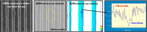 |
| Figure EUV_1: Detailed analysis of a printing pit-type ML-defect missed by state-of-the-art blank inspection. From left to right: printing on wafer on ASML EUV Alpha Demo Tool, not visible on mask scanning electron microscope, top view by atomic force microscopy and cross-sectional view giving indications for its dimensions (estimated ∼70nm wide, ∼4nm deep). |
| The next step is to mitigate such ML-defects. This is the second breakthrough reported here. Together with Zeiss SMS, we have generated experimental proof for the so-called compensation of ML-defects based on the ebeam based MeRiT® repair technology. Such ML-defect cannot be readily repaired, but tweaking the absorber pattern for its presence is shown successful in minimizing the change in printed feature size that it causes. Even if printing ML-defects are found as late as on the printed wafer, we could demonstrate that their impact - at least for those that are marginal for present blank inspection capability - could be minimized by this technique. |
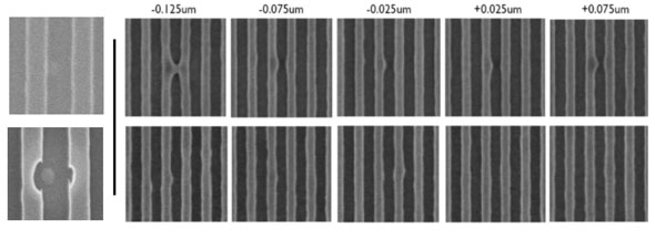 |
| Figure EUV_2: Illustration of successful repair for an ML-defect in a 40nm hp pattern. Top, far left: ML-defect before repair; bottom, far left: after repair; right: through-focus printing behavior on wafer (exposed on ASML EUV Alpha Demo Tool), before repair (top) and after repair (bottom). |
| It remains vital to assure that the critical issue of EUV mask defectivity can be alleviated towards a mature supply of EUV reticles for use in future production of integrated circuits. EUV lithography is considered the preferred solution for 22nm and beyond half-pitch device manufacturing, but its successful application requires this issue to be resolved. |
| Our two breakthroughs have a different merit: the first calls for industry attention towards an improved detection capability, whereas the second provides a solution in case the issue is not solved (in time) at its origin. |
| The demonstration and visualization of printing blank related defects missed during dedicated inspection has been presented at the European Mask and Lithography Conference in Dresden (EMLC 2011) and was honored as the best contribution of the conference |
| Source: imec |

