| Apr 18, 2011 |
Improved bulk FinFET fabrication process |
| (Nanowerk News) Bulk FinFETs are key devices for advanced technology node applications such as analog circuits and SRAMs because of a very good short channel effect control and transistor compactness. Up to now, fin height control and recess of shallow trench isolation (STI) oxide were still critical challenges in the integration of FinFETs. Imec's new fabrication sequence is successfully integrated in a tri-gate FinFET flow to make 20nm wide fins in pitches ranging from 200nm down to 90nm. The process has been demonstrated in a 65nm technology node FET/FinFET co-fabrication flow. The process flow for co-integration uses two oxide field recess steps to finally achieve the target topographies for FinFETs and planar FETs (50nm for FinFETs and flat for planar FETs). |
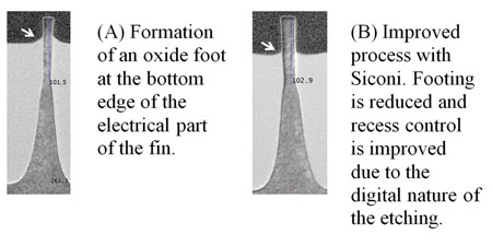 |
| Figure FinFETs_1: HF-based field recess shows oxide footing because the sidewall is covered by thermal oxide which etches slower than the field oxide (A). Siconi™ results in reduced footing because this etching technique is less sensitive to oxide density (B). |
| Morphological and electrical results indicate perfectly filled trenches, better fin height control and bulk FinFET static performance similar to planar CMOS. The availability of such a FET/FinFET co-fabrication flow is attractive for integration of planar CMOS circuits with SRAMs. |
| Improvements in these critical fabrication steps were obtained by adopting the Siconi™ Selective Material Removal (SMR™) chamber of Applied Materials in the fabrication flow. The benefit of this process is the ability to selectively remove silicon oxide in a controlled (digital) manner. |
| The new dry oxide removal process is applied after trench etching (using a carbon/nitride double hard mask approach) and STI trench fill with oxide. In a sequence of steps, a well-controlled amount of oxide (20nm) is consumed in each step, giving a digital character to the etch process. Next, nitride is removed in a hot phosphoric bath and finally the oxide field is recessed until the desired level of fin height is attained. This fin formation method is more robust than conventional wet oxide etch as it has little dependence on the local oxide density variation. Using a wet etch process has the undesirable characteristics of leaving an oxide foot on the fin sidewall and of opening voids in the oxide fill material. |
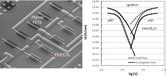 |
| Figure FinFETs_2: (Left) tilted top scanning electron microscopy (SEM) showing planar and FinFET regions after gate patterning and (right) corresponding Id/Vg curves. |
| This work has been presented at the 2011 Ultimate Integration on Silicon (ULIS) Conference, http://www.ulisconference.org. |
| Source: imec |

