| Apr 26, 2011 |
Engineers win patent for protein-based electronic circuits
|
|
(Nanowerk News) University of Arizona engineers have patented a process that could lead to the next big leap in microelectronics, completely changing the way microchips are made.
|
|
The bioengineering breakthrough patented by researchers at the UA College of Engineering is used to build microscopic wiring circuits made of copper insulated by proteins.
|
|
Through a combination of biological processes and electroless copper deposition, the research team has created tiny wires based on proteins called microtubules, aka MTs.
|
|
These tubes have an inner diameter of 15 nanometers and an outer diameter of 25 nanometers and can grow to lengths of several micrometers. Red blood cells have a diameter of about 8 micrometers, a distance in which 320 MTs could be lined up side-to-side.
|
|
The key component of this patent (US 7,862,652 B2) is the ability to deposit copper inside the non-conducting MTs to make tiny insulated wires, said Pierre Deymier, a professor of materials science and engineering and one of the UA faculty members who invented the process.
|
|
Deymier is also director of the School of Sustainable Engineered Systems. Co-inventors include Ian Jongewaard, James Hoying, Roberto Guzman and Srini Raghavan.
|
|
In nature, MTs segregate DNA and chromosomes in a dividing cell. During mitosis (cell division) MTs grow and shrink, appear and disappear, as they are needed. They start forming from a seed protein called a gamma tubulin, Deymier explained.
|
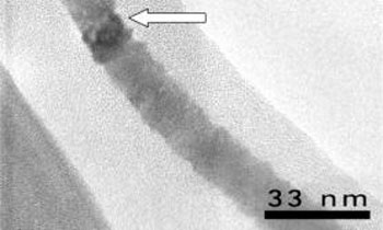 |
| This nanowire was photographed with a transmission electron microscope. The arrow points to the nanowire, which was enclosed in a microtubule. Only the metal wire is showing because electrons from the microscope bombarded the wire when image was made and destroyed the protein. Note the 33-nanometer scale.
|
|
The researchers print gamma tubulins on circuit points where they want wires to start, and print specific peptides on the wires' destinations. Peptides are strands of amino acids, the building blocks of proteins.
|
|
Multiple tubules grow, but only some attach. When all the connections are complete, the solution in which the MTs are growing is changed, and those that aren't attached disappear.
|
|
Next, the remaining MTs are bathed in a copper salt solution. "The key is to metalize the inside of the microtubules before the outside," Deymier said.
|
|
An amino acid called histidine, which has a strong affinity for copper, forms naturally inside the tubules, and the metallization process starts there. By properly timing the copper salt cycle, copper forms only inside the MTs, resulting in tiny insulated wires.
|
|
One of the key breakthroughs was finding a biologically benign deposition process that wouldn't harm MT function or structure. This process was developed by professor Srini Rahavan and his students in the department of materials science and engineering.
|
|
Traditional semiconductor manufacturing technologies are hitting limits in their push for ever-smaller chip features. Biological assembly – growth from the bottom up that mimics the way living organisms are created – offers the processes and control needed to form structures from atoms and molecules, Deymier said.
|
|
These bottom-up technologies promise to be far less expensive, he added. MT-based nanowires are naturally insulated, giving designers more freedom to run wires across one another, something that can't be done with the uninsulated circuit traces found in current chip-printing techniques, such as photolithography.
|
|
In addition to their use in connecting molecule-size circuit elements, MT-based nanowires might be used to extract current from solar cells that mimic photosynthesis, Deymier said. These plant-like photo cells include light-sensitive plant proteins that capture photons and produce electrons. Nanowires could be used to channel these electrons to the outside world.
|
|
The next step is to apply this nanowire research to devices and manufacturing processes. Said Deymier: "We would be happy to see people license this technology to develop microchip manufacturing processes or any other related processes."
|

