| May 16, 2011 |
Looking inside nanomaterials in three dimensions |
| (Nanowerk News) On May 13th 2011, the journal Science published a paper where scientists from Risø DTU in collaboration with scientists from China and USA, report a new method for revealing a 3D picture of the structure inside a material ("Three-Dimensional Orientation Mapping in the Transmission Electron Microscope"). |
| Most solid materials are composed of millions of small crystals, packed together to form a fully dense solid. The orientations, shapes, sizes and relative arrangement of these crystals are important in determining many material properties. |
 |
| Traditionally, it has only been possible to see the crystal structure of a material by looking at a cut surface, giving just 2D information. In recent years, x-ray methods have been developed that can be used to look inside a material and obtain a 3D map of the crystal structure. However, these methods have a resolution limit of around 100nm (one nanometer is 100,000 times smaller than the width of a human hair). |
| In contrast, the newly developed technique now published in Science, allows 3D mapping of the crystal structure inside a material down to nanometer resolution, and can be carried out using a transmission electron microscope, an instrument found in many research laboratories. |
| Samples must be thinner than a few hundred nanometers. However, this limitation is not a problem for investigations of crystal structures inside nanomaterials, where the average crystal size is less than 100 nanometers, and such materials are investigated all over the world in a search for materials with new and better properties than the materials we use today. |
| For example, nanomaterials have an extremely high strength and an excellent wear resistance and applications therefore span from microelectronics to gears for large windmills. The ability to collect a 3D picture of the crystal structure in these materials is an important step in being able to understand the origins of their special properties. |
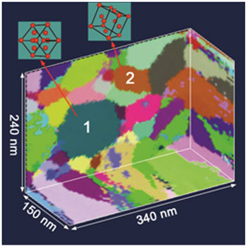
| An example of such a 3D map is given in the figure, showing the arrangement of crystals in a 150nm thick nanometal aluminium film. The crystals have identical lattice structure (arrangement of atoms) but they are orientated in different ways in the 3D sample as illustrated by the labels 1 and 2. The colours represent the orientations of the crystals and each crystal is defined by volumes of the same colour. The individual crystals of various sizes (from a few nm to about 100 nm) and shapes (from elongated to spherical) are clearly seen and mapped with a resolution of 1 nanometer. |
| An important advantage of such 3D methods is that they allow the changes taking place inside a material to be observed directly. For example, the mapping may be repeated before and after a heat treatment revealing how the structure changes during heating. |
| This new technique has a resolution 100 times better than existing non-destructive 3D techniques and opens up new opportunities for more precise analysis of the structural parameters in nanomaterials. |
| Source: Risø National Laboratory for Sustainable Energy |

