| May 19, 2011 |
Seeing an atomic thickness |
| (Nanowerk News) Scientists from National Physical Laboratory (NPL), in collaboration with Linköping University, Sweden, have shown that regions of graphene of different thickness can be easily identified in ambient conditions using Electrostatic Force Microscopy (EFM). |
| The exciting properties of graphene are usually only applicable to the material that consists of one or two layers of the graphene sheets. Whilst synthesis of any number of layers is possible, the thicker layers have properties closer to the more common bulk graphite. |
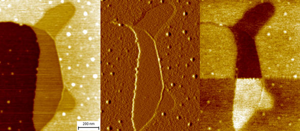 |
| The left hand image is the topography; the middle the topography error image; and right the electrostatic force microscopy image where the tip bias has been switched half way through the image. |
| For device applications one- and two-layer graphene needs to be precisely identified apart from the substrate and regions of thicker graphene. Exfoliated graphene sheets up to ∼100 µm in size can be routinely identified by optical microscopy. However, the situation is much more complicated in the case of the epitaxial graphene grown on silicon carbide wafers with a diameter up to 5 inches where the straightforward identification of the graphene thickness is difficult using standard techniques. This research shows that EFM, which is one of the most widely accessible and simplest implementations of scanning probe microscopy, can clearly identify different graphene thicknesses. The technique can also be used in ambient environments applicable to industrial requirements. |
| This work was recently published in Nano Letters ("Mapping of Local Electrical Properties in Epitaxial Graphene Using Electrostatic Force Microscopy"). |
| Source: National Physical Laboratory |

