| Jun 07, 2011 |
New chemical method paves the way for making a greater variety of light-sensitive materials that was not possible before |
| (Nanowerk News) Scientists from Singapore's Institute of Materials Research and Engineering (IMRE) and National University of Singapore (NUS) have created a new chemical method that enables the development of a variety of tiny light conducting metal-semiconductor contacts. These light-sensitive nano-sized components could help create bioimaging labels as well as better photocatalysts used in fuel cells. |
| Sticking a ball onto a small pole might seem simple but try doing that at a scale a billion times smaller. Researchers have been making 'matchstick-like' nano-sized metal ball-semiconductor pole features with light-sensitive properties for some time but with great difficulty and strict limitations on the type of metals that can be used. The 'matchstick-like' shape is used because the ends of a semiconductor pole have been found to be more chemically reactive compared to other shapes thus allowing metals to be deposited easier. |
| Scientists from IMRE and NUS have recently discovered a chemical process that is not only simpler to perform but greatly expands the range of different metals that can be coupled with the semiconductors ("Light-Induced Selective Deposition of Metals on Gold-Tipped CdSe-Seeded CdS Nanorods"). This opens the way for nano-sized structures with enhanced photoconductive properties or with entirely new functions. For example, the new nanostructures chemically synthesised by the researchers may be further developed as labels for enhanced bio-imaging applications such as magnetic resonance imaging (MRI), fluorescence and dark field imaging. |
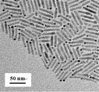 |
| Metal-semiconductor 'matchstick-like' structures viewed under high-powered transmission electron microscopy. |
| Referring to the possibility of the nanostructures being used to enhance current bioimaging techniques, Dr Chan Yin Thai, an IMRE scientist, explained, "The breakthrough may allow multiple imaging modes to be supported by a single label, which can significantly improve current imaging capabilities and give rise to powerful diagnostic tools". |
| The light-sensitive metal-semiconductor pole features also have intrinsically good photocatalytic properties, where chemical reactions are triggered by light. For the moment, the researchers are looking at using the new method to produce materials that have 'green' photocatalytic applications, for instance, materials that enhance water-splitting to produce hydrogen more efficiently for fuel cells; and materials that actively degrade environmental pollutants on exposed surfaces like buildings and cars. |
| "The development of metal-semiconductor nanostructures for use in devices is still in its infancy but having access to a large variety of different metals really opens doors to a vast number of possibilities for scientific exploration and is a crucial milestone for ensuring continued R&D," Dr Chan explained. |
| The scientists used a novel approach to develop the new method – by exploiting the light-sensitive properties of the semiconductor 'pole'. By putting gold particles onto the 'pole' and then treating it with UV light, the IMRE and NUS scientists discovered that this made it easier to attach a greater variety of metals, using only mild chemicals. Before the success of this research, the metals that could be used for the 'ball' were limited. The chemicals needed in conventional treatment had to be mild so that it would not degrade the semiconductor 'pole'. The degradation of the 'pole' would affect the photocatalytic properties of the structure. This limited the variety of metals that could be used as tougher metals could not be fixed onto the 'pole' using the mild chemicals. |
| Source: A*STAR |

