| Jun 13, 2011 |
Resistive memory built with exposed, planar nanowires provides insights into resistive switching |
| (Nanowerk News) The current standard for non-volatile or 'flash' memory involves relatively complex structures. Much simpler is resistive memory, which consists of a single continuous strip of material between metal electrodes. The resistance across this material is forced low or high by applying 'set' or 'reset' voltages. |
| Resistive memory is known to rely on the formation and destruction of nanoscale, filamentary conductive pathways between the electrodes. However, the exact nature of these pathways is not completely understood, particularly for materials in which positive charge carriers are responsible for conduction, known as 'p-type' materials. Takeshi Yanagida, Tomoji Kawai and colleagues at Osaka University in Japan and Konkuk University in Korea have now revealed key details of resistive switching in p-type devices ("Intrinsic Mechanisms of Memristive Switching"). |
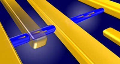 |
| Schematic illustration of a resistive memory device consisting of exposed cobalt oxide nanowires (blue) and gold electrodes (gold). (© 2011 ACS) |
| The researchers were able to gather a unique set of data by studying a novel device structure. Most resistive memory elements are constructed as thin-film capacitors with a flat sheet of resistive switching material covered by metal electrodes on both sides. Building on their own previous work, the researchers instead constructed a planar device in which the resistive switching material, cobalt oxide, was formed into a single, exposed nanowire, allowing characterization that would not otherwise be possible. |
| The team observed that exposing their nanowire devices to oxidizing gases resulted in increased currents, indicating that positive carriers were responsible for conduction. By constructing field-effect transistors in which the nanowire formed the channel, they observed that increasing the gate voltage reduced the current. This, too, indicated that the current was carried by positive carriers. Finally, they measured the resistance between the nanowire midpoints and the cathode, as well as between the midpoint and the anode, and found that the resistance on the cathode side was larger. |
| Taken together, the data suggest that the application of a high 'set' voltage causes oxygen ions to migrate towards the cathode of a p-type resistive memory device, establishing a conducting pathway made up of cation vacancies concentrated near the cathode. This model contradicts previous studies in which it was concluded that oxygen vacancies near the anode were responsible for switching. This new model should be broadly applicable, says Yanagida, advancing the prospects for practical, ultrahigh-density nonvolatile memory technologies. |
| Source: Tokyo Institute of Technology |

