| Jun 27, 2011 |
Organic electronics: Peel carefully |
| (Nanowerk News) Graphene sheets eluded detection for many years until the relatively recent discovery of a decidedly low-tech approach for isolating them. By fixing flakes of graphite between two pieces of adhesive tape and then pulling the layers apart, researchers were able to split the graphite into thinner and thinner layers, eventually giving an isolated sheet of atomically thick graphene. Now, a team led by Xiaodong Chen and Christian Kloc from Nanyang Technological University in Singapore has found that this sticky exfoliation technique can help advance the burgeoning field of organic electronics ("Ultrathin organic single crystals: fabrication, field-effect transistors and thickness dependence of charge carrier mobility"). |
| Replacing silicon-based field-effect transistors (FETs) with organic semiconductors would allow manufacturers to do away with difficult, expensive clean-room procedures in favor of roll-to-roll printing on cheap, flexible substrates. However, current organic-based devices are constructed by depositing thin films of organic materials, which are prone to defects and dislocations that hinder charge carrier mobility and impede device performance. Pure, single organic semiconductor crystals, on the other hand, could provide higher performance and greater mobility than thin films, but are difficult to fabricate consistently. |
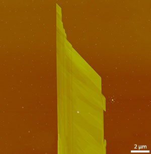 |
| An atomic force microscopy image of a F16CuPc crystal mechanically exfoliated into an extremely thin sheet using adhesive tape. |
| As the thickness of organic crystals has emerged as a primary factor affecting charge mobility in such organic semiconductor crystals, Chen, Kloc and their co-workers set out to make crystals of the organic semiconductors F16CuPc and pentacene as thin as possible using the adhesive tape method. The layered structures of these crystals make them "perfect for splitting", according to Kloc. The team's organic crystal cleavage technique yielded large-sized, flexible crystals of a few monolayers to a few micrometers in thickness (see image). |
| Experiments with the exfoliated organic crystal-based FETs demonstrated that crystal thicknesses below a few hundred nanometers significantly boosted charge carrier mobility, in some cases by two orders of magnitude. Kloc notes that at these dimensions, the measured mobility approaches its true, intrinsic value instead of an extrinsic value dominated by processing conditions — a finding that should advance the development of devices like organic solar cells. |
| The team expects that thinning the crystals down even further to atomic levels could yield results that are even more surprising. "This technique may bridge the fields of organic microelectronics and molecular electronics," says Kloc. |
| Source: Tokyo Institute of Technology |

