| Jun 30, 2011 |
Innovative approaches for patterning and doping graphene |
| (Nanowerk News) The chemical synthesis of graphene is considered as an efficient means of mass producing graphene-based compounds. Typically, the chemical process of producing graphene consists of first chemical exfoliation of graphite to produce graphene oxide (GO) flakes, followed by the reduction of the GO, which yields graphene flakes. |
| Now in spite of the proliferation of chemical approaches for the synthesis there are still two fundamental issues to resolve. First is the development of protocols for integrating chemical synthesis with device fabrication technology, namely, methods for the positioning GO or graphene flakes at specific locations on substrates to enable photolithography and device fabrication, without having to 'hunt' for graphene. The second issue is an effective and controlled means of doping graphene in solution—again an important factor for real life applications of this material. |
| Here in two recent publications, Adarsh Sandhu at Toyohashi University of Technology and colleagues demonstrate novel approaches to resolve the issues of device patterning and doping of graphene. |
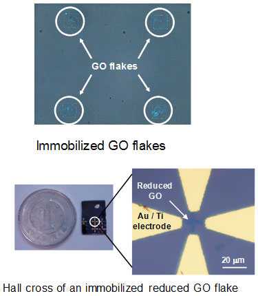 |
| Immobilization and device fabrication of GO flakes. |
| In JJAP Adarsh Sandhu and his doctoral student Ryousuke Ishikawa describe a straightforward process for positioning individual flakes of graphene oxide at specific locations of a substrate and subsequent fabrication of device structures using individual flakes of chemically derived graphene ("Patterning of Two-Dimensional Graphene Oxide on Silicon Substrates"). Notably, the researchers exploited the negatively charged surface of GO flakes, and successfully patterned GO flakes onto photolithographically defined positively charged regions on silicon substrates. The immobilized GO flakes were reduced in a saturated vapor of hydrazine monohydrate at 80°C for 18 hours and post-annealing in vacuum. Electrical measurements using photolithographically defined Hall crosses showed the monolayer films of reduced GO films to have a carrier concentration and mobility of 1011 cm-2 and 10 cm2/Vs, respectively. |
| In addition, the researchers addressed the issue of doping in Nanoscale Research Letters ("Doping graphene films via chemically mediated charge transfer"), where they describe an inexpensive method of producing chemically derived graphene-based transparent conducting films (TCFs) via charge transfer by conjugated organic molecules. In this approach, the process of GO reduction and carrier doping were carried out in liquid phase, that is, without the use of vacuums, which is an advantage for mass production of doped graphene of touch panel displays and solar cell panels. |
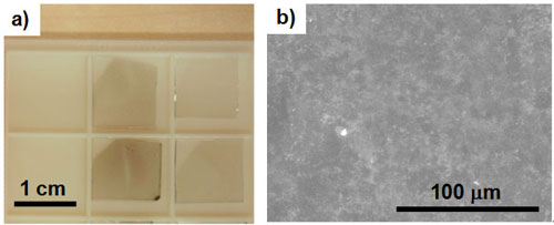 |
| Graphene films on glass substrate. (a) Photograph and (b) SEM image. |
| GO films produced by Hummer's method were reduced to form graphene by dispersing GO into an aqueous solution containing N2H4, a strong reductant (with NH3 to adjust pH) in a water bath at 95°C water bath for 1 h, when the and the color of the dispersion changed from brownish color to gray. Finally, the solvent of reduced graphene oxide (RGO) dispersion was replaced by N,N-dimethylformamide (DMF) using an evaporator. |
| Doping graphene via charge transfer by tetracyanoquinodimethane (TCNQ)—well-known as a powerful electron accepter, which is expected to favor electron transfer from graphene into TCNQ molecules, thereby leading to p-type doping of graphene films—molecules. Importantly, small quantities of TCNQ drastically improved the resistivity without degradation of optical transparency. |
| Source: Toyohashi University of Technology |

