| Jul 20, 2011 |
A closer look at plasmonics |
| (Nanowerk News) Surface plasmon resonance—the collective oscillations of charges on the surfaces of metals—is the basis of operation for a wide range of sensing, imaging and photonics devices. Scientists commonly use plasmon hybridization theory to simulate the various modes of surface plasmon resonance in metallic nanostructures, but experimental verification of the results remains a challenge. Joel Yang and co-workers at the A*STAR Institute of Materials Research and Engineering in collaboration with colleagues from Imperial College London in the UK have now developed a strategy for characterizing the full spectrum of surface plasmon modes in complex nanostructures ("High-Resolution Mapping of Electron-Beam-Excited Plasmon Modes in Lithographically Defined Gold Nanostructures"). |
| The researchers constructed gold nanostructures on a silicon nitride membrane by electron beam lithography. They then used transmission electron microscopy in combination with electron energy-loss spectroscopy (EELS)—a high-resolution, electron beam-based technique for determining the structural, chemical and electronic properties of a material—to probe the plasmonic properties of the nanostructures in detail. |
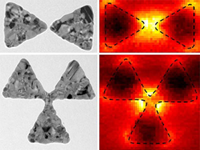 |
| Electron microscopy images (left) of gold nanostructures and EELS images (right) showing their plasmon modes (gradient denotes electric field intensity). (© 2011 ACS) |
| Using this approach, the researchers were able to determine the location and energy of surface plasmon modes in various configurations of gold nanostructures. Significantly, they were able to map the full spectrum of surface plasmon modes—even modes that did not interact with light, so called 'dark plasmons'. |
| Yang and his co-workers tested their strategy on connected and disconnected triangles, each about 100 nanometers to a side, as a proof of principle. They found that plasmon modes at the vertices differ from those at the edges of the triangle (see image). They also observed that modes in widely separated 'dimers' and 'trimers'—comprising pairs and triplets of triangles—changed as the triangles were brought together. |
| Dark plasmon modes, in particular, were concentrated in the gap between the triangles of dimers and trimers. In dimers, the dark modes had similar energies to bright modes, making then difficult to observe without EELS. This similarity may also explain previously observed features of the fluorescence of molecules placed in the gap between pairs of metallic nanostructures. |
| The data collected were successfully described with a relatively simple numerical model. Yang says the results demonstrate how useful the combination of transmission electron microscopy and EELS is for probing and measuring surface plasmons. "Probing nanostructures with a localized electron beam in EELS is like hitting a drum with a drum stick, bringing out many different 'tones' of plasmon resonance," says Yang. "This allows us to see resonances that are not usually considered, and should help us design and build better plasmonic devices." |
| Source: A*STAR |

