| Aug 11, 2011 |
Structural consequences of nanolithography |
| (Nanowerk News) Users from the University of Wisconsin-Madison and the Center for Nanophase Materials Science, working with the X-Ray Microscopy Group, have discovered structural effects accompanying the nanoscale lithography of ferroelectric polarization domains. The results shed new light on the physics of structural changes induced during this model nanoscale lithographic process ("Structural Consequences of Ferroelectric Nanolithography"). |
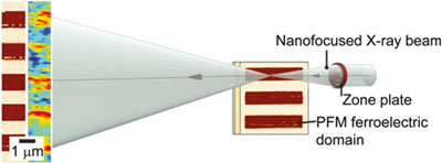 |
| Ferroelectric domains written by PFM exhibit a subtle structural distortion that can be directly observed using hard X-ray nanodiffraction microscopy. |
| Developing the means to manipulate nanoscale patterns at their fundamental length scales has led to tremendous growth in the applications of scanning probe lithography. The potential of these capabilities has not yet been fully realized, in part because the large number of sometimes subtle physical processes involved have not yet been sufficiently well described. X-ray nanodiffraction microscopy performed at the Hard X-Ray Nanoprobe beamline was used to probe a pattern written into a ferroelectric layer by using scanning-probe ferroelectric nanolithography. This adaptation of piezoresponse force microscopy (PFM) can be used to write arbitrary nanoscale domain patterns into a ferroelectric thin film. The stable strain pattern observed shows the overall shape of the film is unchanged, but the electrical polarization is modified. |
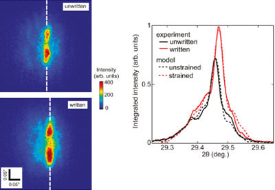 |
| Modeling shows that the writing process induces a structural electromechanical response to unscreened charges at surfaces and interfaces, altering the local free energy of written ferroelectric domains. |
| The ferroelectric lithography approach is one of a number of emerging ways to control nanoscale degrees of freedom with scanning probes, which in other systems also can provide control of magnetic and charge-ordered domains. The researchers found that a crystallographic distortion in the lattice of the ferroelectric Pb(Zr,Ti)O3 (PZT) thin film arises from the nanoscale electromechanical response to unscreened charges at surfaces and interfaces. The resulting increase in the free energy of written domains inferred from this poses an important limit for ferroelectric nanolithography. Based on this insight, it will be possible to extend the capability of PFM and other nanoscale patterning methods using direct local structural information. |
| Source: Argonne National Laboratory |

