| Aug 22, 2011 |
Selective CVD growth of GeSn: a new approach for implementing stress in Ge based MOSFETs |
| (Nanowerk News) Imec reports for the first time selective chemical vapor deposition (CVD) of GeSn in a production-like environment using commercially available Ge and Sn precursors. The resulting GeSn layers with 8% Sn are defect free, fully strained and thermally stable for temperatures up to 500°C. This technique is used to implement uniaxial compressive stress in a Ge channel, the key method for reaching very high mobility values in MOSFETs. |
| Ge as a high mobility channel material has attracted much interest for future CMOS applications where it could potentially replace Si in pMOSFETs. High mobility values can be obtained by stress engineering in the Ge channel. Imec now presents an innovative concept for implementing uniaxial compressive stress in Ge channels by boron doped selective epitaxial growth of GeSn CVD in embedded source/drain areas*. The technique has been demonstrated in a 200mm production-like environment, and is expected to be easily transferable into a 300mm environment. |
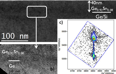 |
| Cross-section TEM and 224 XRD-RSM of fully strained defect-free GeSn layers grown on a Ge substrate. |
| Key of this technique is a new approach for growing GeSn in a CVD environment. CVD growth of GeSn has so far only been reported by using SnD4 as a Sn gas precursor, but the instability of this precursor restricts the applicability of the technique. Imec uses the stable SnCl4 and Ge2H6 as commercially available Sn and Ge precursors respectively. This permits the growth of GeSn layers on a Ge surface with Sn content up to 8%. |
| As shown by transmission electron microscopy (TEM), no defects are found in the 40nm GeSn layer and according to x-ray diffraction reciprocal space mapping (XRD-RSM) measurements, the layer is fully strained. The GeSn layer grown with this approach survives to further thermal treatments at temperatures up 500°C (for 10 minutes). In addition, in-situ boron (B) doped GeSn CVD growth was investigated by using a combination of Ge2H6, SnCl4 and B2H6 precursors. B was found to be 100% electrically active in GeSn:B layers grown with a B concentration of 1.7e19cm-3. |
| The CVD grown GeSn layer can also be used as a high-mobility channel material on Ge. A strained GeSn channel on Ge is a possible candidate to be used in the device channel of future Ge based MOSFET devices. In this work, first working GeSn capacitors were realized by depositing Al2O3 on the CVD grown GeSn layers**. |
| The CVD growth of GeSn with commercially available precursors will boost the research on high-mobility MOSFETs. Besides, it opens new routes for group-IV semiconductors research in other fields, such as photonics (having indirect-to-direct-bandgap transition expected for about 10% Sn incorporated in monocrystalline GeSn allys) and photovoltaics (ternary SiGeSn alloys). |
| More detailed results can be found in *B. Vincent et al., Microelec. Eng. 88 (2011) 342 and in **B. Vincent et al., Electrochem. Soc. Trans. 2011 (accepted for publication). |
| Source: imec |

