| Aug 24, 2011 |
New x-ray technique to probe deep below material surfaces should be boon for nanodevices
|
|
(Nanowerk News) The expression "beauty's only skin-deep" has often been applied to the chemistry of materials because so much action takes place at the surface. However, for many of the materials in today's high technologies, such as semiconductors and superconductors, once a device is fabricated it is the electronic structures below the surface, in the bulk of the material or in buried layers, that determine its effectiveness. For the past 30 years, one of the most valuable and widely used techniques for studying electronic structures has been ARPES – Angle-Resolved PhotoEmission Spectroscopy. However, this technique primarily looks at surfaces. Now, for the first time, bulk electronic structures have been opened to comparable scrutiny through a new variation of this standard called HARPES – Hard x-ray Angle-Resolved PhotoEmission Spectroscopy – whose development was led by researchers with the U.S. Department of Energy (DOE)'s Lawrence Berkeley National Laboratory (Berkeley Lab).
|
|
"HARPES should enable us to study the electronic structure of any new material in the bulk, with minimum effects of surface reactions or contamination," says physicist Charles Fadley who led the development of HARPES. "Our technique should also allow us to probe the buried layers and interfaces that are ubiquitous in nanoscale devices, and are key to smaller logic elements in electronics, novel memory architectures in spintronics, and more efficient energy conversion in such technologies as photovoltaic cells."
|
|
Fadley is a physicist who holds joint appointments with Berkeley Lab's Materials Sciences Division and the University of California (UC) Davis where he is a Distinguished Professor of Physics. He is also one of the world's foremost practitioners of photoelectron spectroscopy, a technique based on the photoelectric effect described in 1905 by Albert Einstein. When a beam of photons — particles of light such as x-rays – is flashed on a sample, energy is transferred from the photons to electrons, causing them to be emitted from the sample. By measuring the kinetic energy of these emitted photoelectrons and the angles at which they are ejected, scientists can learn much about the sample's electronic structure.
|
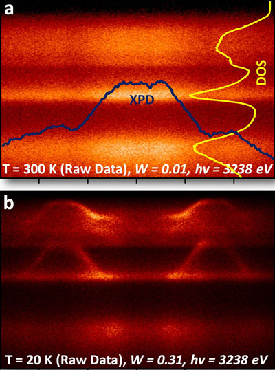 |
| By collecting and comparing HARPES data at room and cryo temperatures, Berkeley Lab researchers were able to correct for density of state (DOS) and x-ray photoelectron diffraction (XPD) influences in determining electronic structures deep below sample surfaces. (Image from Fadley group)
|
|
The successful demonstration of the HARPES technique has been reported in the journal Nature Materials in a paper titled ("Probing bulk electronic structure with hard X-ray angle-resolved photoemission"). Fadley was the senior author of this paper. The lead and corresponding author was Alexander Gray, a member of Fadley's UC Davis research group and also an affiliate with Berkeley Lab's Materials Sciences Division.
|
|
"The key to probing the bulk electronic structure is using hard x-rays, which are x-rays with sufficiently high photon energies to eject photoelectrons from deep beneath the surface of a solid material," Gray says. "High-energy photons impart high kinetic energies to the ejected photoelectrons, enabling them to travel longer distances within the solid. The result is that more of the signal originating from the bulk will be detected by the analyzer."
|
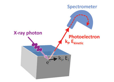 |
| With photoemission spectroscopy techniques, such as HARPES, a beam of x-rays flashed on a sample transfers energy from the photons to electrons, causing photoelectrons to be emitted. Measuring the kinetic energy of these photoelectrons and the angles at which they are ejected reveals much about the sample's electronic structure. (Image from Fadley group)
|
|
Whereas the typical ARPES experiment, using low energy or "soft" x-rays (10~100 eV photons), probes to a depth of less than 10 angstroms (a few layers of atoms), with their HARPES technique Fadley and Gray and their colleagues on this project were able to probe as deep as 60 Angstroms into the bulk of single crystals of tungsten and gallium-arsenide. Their achievement was made possible by a combination of third generation light sources capable of producing intense beams of hard x-rays, and an advanced electron spectrometer to measure energies and angles.
|
|
"While high-energy photons are needed to penetrate into the bulk, at high energies the photoemission intensity that carries information about the electronic band structure is drastically reduced by various factors, such as phonon effects and small photoelectric cross sections of the valence-band electron orbitals," Gray says. "However, HARPES measurements become possible with the advent of the third-generation synchrotron light sources and the development of hard x-ray monochromators and optics capable of focusing a highly intense x-ray beam into a very small measurement spot."
|
|
To demonstrate the capabilities of their HARPES technique, Fadley and Gray used a high intensity undulator beamline at the SPring8 synchrotron radiation facility in Hyogo, Japan, which is operated by the Japanese National Institute for Materials Sciences. The samples they worked with, tungsten and gallium arsenide, contain relatively heavy elements that have relatively small phonon effects (atomic vibrations) but to further reduce these effects the samples were cryo-cooled. By combining room temperature and cryo data, the researchers were able to correct for the influence of indirect transitions and photoelectron diffraction in their results.
|
|
"Having sufficient photons from the beamline was critical as was having a high energy resolution that required an undulator source and a special monochromator and a photoelectron spectrometer with both high throughput for intensity and a lens with angle-resolving capability," Fadley says.
|
|
Adds Gray, "Our HARPES technique not only provided us with information about the energies of the emitted photoelectrons, but also with information about the crystal momentum of electrons within the bulk solid. This extra dimension carries a vast amount of information regarding electronic, magnetic and structural properties of materials, and can be used for in-depth studies of such novel phenomena as high-temperature superconductivity and so-called Mott transitions from insulating to conducting states that might be used for logic switching in the future."
|
|
In the future, Fadley and Gray will be able to carry out HARPES experiments much closer to home. At Berkeley Lab's Advanced Light Source (ALS), the first of the world's third generation synchrotron radiation facilities, a new experimental chamber for beamline 9.3.1 is scheduled to open this fall that will provide unique hard x-ray angle-resolved photoemission capabilities.
|
|
Says Zahid Hussain, who manages the ALS Scientific Support group, "An additional hard x-ray photoemission spectroscopy chamber at beamline 9.3.1 will feature an ambient pressure high energy photoemission capability that will allow the study of energy related problems, such as batteries, fuel cells, and catalysis under in-situ and in-operando conditions. It will also enable depth-sensitive studies and make it possible to probe not only solid, but also gas and liquid interfaces. This will be the first such experimental facility in the world."
|

