| Sep 21, 2011 |
New gallium nitride transistor technology - faster, smaller and more economical
|
|
(Nanowerk News) For the first time, researchers from CNRS France and ETH Zurich have succeeded in producing high-performance high-electron-mobility transistors (HEMTs) made of gallium nitride (GaN) on a silicon(110) wafer. This makes these transistors compatible with current complementary metal oxide semi-conductor (CMOS) chips based on silicon of the same crystal orientation ("RF Performance of AlGaN/GaN High-Electron-Mobility Transistors Grown on Silicon (110)").
|
|
CMOS chips are generally produced on silicon wafers with the so-called (100) or (110) crystal orientation. GaN, on the other hand, could previously only be used on (111)-silicon until now. This new development makes it possible to construct hybrid electronic components that combine the computational power of the CMOS chip and the power handling capability of GaN transistors, which means power electronics can be made even more compact.
|
|
Transistors are used in high-voltage circuits, for computation, and to amplify electrical radio-frequency signals. Until now they have predominantly consisted of silicon. However, electrical engineers recently began to exploit the advantages of gallium nitride for the construction of power electronics to develop faster, heat-resistant and above all energy-efficient transistors.
|
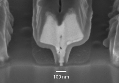 |
| For the first time, researchers from CNRS France and ETH Zurich have succeeded in producing high-performance high-electron-mobility transistors (HEMTs) made of gallium nitride (GaN) on a silicon(110) wafer. (Photo: of C. Bolognesi / ETH Zürich)
|
|
Silicon substrates reduce price of nitride technology
|
|
Gallium nitride technology was once deemed too expensive to replace silicon technology. However, researchers such as Bolognesi and his French colleagues are succeeding in growing gallium nitride on a silicon wafer, which makes the technology more economical. For the substrate, they used pure silicon with a specific crystal orientation. Known as silicon(110), the substrate costs around fifty cents per square centimetre, which is much cheaper than the usual substrates, sapphire or silicon carbide (SiC), which cost about five dollars, or even twenty dollars/cm2 in the case of SiC. Moreover, using silicon, large wafers measuring thirty centimetres in diameter can be produced, which is not possible with sapphire and SiC. However, because GaN and silicon have different material properties, it is difficult to combine the two materials on a wafer; cracks may form during heating, for instance, as the materials expand to a different degree. However, Colombo Bolognesi's French research colleagues have now found ways to grow GaN on silicon(110) and get around the problem.
|
|
"Most transistors in the world are still based on silicon," says Bolognesi. This semiconductor does not just serve as a substrate, but also the base material of transistors and chips. "Pretty much everything in electronics is still made of silicon. It's a fabulous material," confirms the ETH Zurich professor; "God's gift to engineers."
|
|
However, silicon also has its drawbacks. At high temperatures above 200°C silicon-based components begin to malfunction. Gallium nitride transistors, on the other hand, can withstand temperatures of up to 1000°C, which makes the material attractive for building sensors in car engines, for example. Moreover, GaN can withstand electrical fields that are up to fifteen times stronger than in silicon; the electrons also move more quickly in GaN than in silicon, which enables faster circuitry. "This is especially important for telecommunications since the information is processed more rapidly and efficiently," says Bolognesi.
|
|
Nitride technology curbs energy wasting
|
|
Thanks to its heat resistance, power electronics made of GaN barely requires cooling. If the base stations of mobile communications installations were equipped with GaN transistors, for instance, the providers would not need power-guzzling cooling systems. Moreover, conventional base stations require ten kilowatts input to emit just one kilowatt. "A lot of energy is thus wasted, which ultimately costs the environment and consumers dearly," says Bolognesi. If silicon electronics were to be replaced with GaN-Si electronics, a lot of energy could be saved. As far as the ETH-Zurich professor is concerned, gallium nitride is therefore just the ticket for use in many areas of electronics, especially power electronics.
|
|
Moreover, GaN could help save energy in lighting, which is currently responsible for a fifth of the global electricity consumption. A five-watt LED lamp based on GaN, however, generates the same amount of light as a conventional sixty-watt bulb, which makes enormous energy savings possible, stresses Bolognesi.
|
|
The same also goes for voltage conversion in appliances. When you plug a PC into a 230-volt socket, a converter inside the appliance provides the right voltage to the chips; such converters can be more efficient with GaN technology. Experts estimate that the global energy consumption could be reduced by a quarter if the energy were used intelligently at the place of consumption.
|
|
What is more, GaN transistors have shown to be lightning-fast and allow frequencies of up to 205 gigahertz – more than enough to make computers, mobile phones, and power electronics quicker, smaller and more economical.
|
|
Changeover costs money
|
|
"Technically speaking, everything is there to help this technology make a break through. What's lacking is an industrial partner that wants to launch gallium nitride silicon electronics on the market," says the ETH-Zurich professor. Just why telecommunications companies did not already convert to GaN technology is clear for Bolognesi: "The conversion costs money." In the ideal scenario, silicon components could be replaced with GaN power electronics when required. Consequently, Bolognesi hopes that support for the changeover will come from the political arena: introducing a strict CO2 emission guidelines, for instance, would encourage companies to reduce their energy costs. This would incite telecommunications companies for example to invest in greener technologies and to reduce CO2 emissions.
|

