| Sep 21, 2011 |
Researchers get first detailed look at nitrogen doping in single-layer graphene
|
|
(Nanowerk News) The strength, flexibility, transparency and high electrical conductivity of single-layer graphene make it a potentially unique and valuable material for the next generation of electronic devices. Made of carbon atoms arranged in a honeycomb pattern – think of a chicken-wire fence – it is 97 percent transparent and 1,000 times stronger than steel.
|
|
Researchers are working on ways to tune the properties of graphene for specific electronic applications. One way to do that is by doping – introducing small amounts of other elements, such as nitrogen or phosphorus, that either add or subtract electrons from the system. Widely used in silicon technology, doping has been carried out experimentally in single-layer graphene sheets; but until now, the details of how the dopant atoms fit into the sheet and bond with their carbon neighbors remained elusive.
|
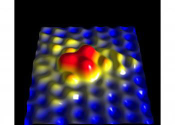 |
| A close-up, three-dimensional image of a single nitrogen atom in a sheet of graphene – a material made of carbon atoms arranged in a honeycomb pattern. The larger nitrogen atom sticks out above its carbon neighbors and contributes about half of its extra electron to the graphene lattice, changing its electronic properties. The image was made with a scanning tunneling microscope.
|
|
In a study reported Aug. 9 in Science ("Visualizing Individual Nitrogen Dopants in Monolayer Graphene"), researchers from Columbia University, Sejong University in Korea and SLAC and Brookhaven national laboratories used a combination of four techniques to make the first detailed images of nitrogen-doped graphene film. They showed that individual nitrogen atoms had taken the places of carbon atoms in the two-dimensional sheet; that about half of the extra electron contributed by each nitrogen atom was distributed throughout the graphene lattice; and that this changed the electronic structure of the graphene sheet only within a short distance – about the width of two carbon atoms – from the dopant atoms. The ability to control the electronic structure at the atomic level has important implications for tuning the unique electronic properties of graphene for particular device applications.
|
|
"We're not trying to work on existing systems and make them better. We're looking for new directions that can potentially enable much higher efficiencies," said paper co-author Theanne Schiros, a surface scientist at the Department of Energy's Energy Frontier Research Center at Columbia, who is investigating graphene as a possible electrode for novel photovoltaic devices.
|
|
"Now we see that doping is a strategy that can be applied to graphene cleanly and robustly," she said, providing a potential way to create high-quality graphene films for use in electronic applications, including solar cells.
|
|
Schiros is no stranger to SLAC, having done her Ph.D. work here under Anders Nilsson. Her current work at Columbia focuses on using X-rays from synchrotron light sources to probe novel materials for use in renewable energy technologies.
|
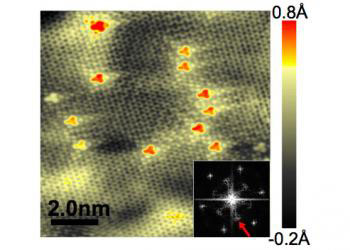 |
| This image shows an area of graphene that's been doped with atoms of nitrogen. Tiny red spots show single atoms of nitrogen that have settled into the graphene lattice; since they're a bit larger than carbon atoms, they stick out slightly above it. Larger spots are clusters of nitrogen atoms. The image was made with a scanning tunneling microscope.
|
|
For this study, she returned to SLAC to work with Dennis Nordlund, a staff scientist at SLAC's Stanford Synchrotron Radiation Lightsource (SSRL), where recent upgrades allowed them to automatically scan many samples of the nitrogen-doped graphene films at once.
|
|
The research team grew the films by depositing chemical vapor on a thin sheet of copper foil.
|
|
They analyzed some samples of film while it was on the copper foil, and transferred others to silicon dioxide, the standard substrate for device measurements, for testing. Each sample was examined with Raman spectroscopy and scanning tunneling microscopy (STM) at Columbia, and with X-ray beams at SLAC's SSRL, and Brookhaven's National Synchrotron Light Source (NSLS).
|
|
The Raman spectra showed that the nitrogen dopant had changed the electronic properties of the graphene sheet without disturbing its basic structure. X-ray measurements at SSRL beamlines 10-1 and 13-2 and NSLS beamline U7A indicated that the nitrogen atoms lay within the plane of the graphene sheet and had each bonded with three carbon neighbors; in other words, each nitrogen atom had replaced a carbon in the sheet.
|
|
Finally, the STM images showed the nitrogen atoms as bright spots on the graphene surface. By counting those spots, the researchers determined that the concentration of nitrogen dopant per carbon atom varied from .23 to .35 percent. The images also revealed that the nitrogen atoms stuck out from the graphene layer by about .6 Ångstrom, as they would if they had substituted for carbon in the lattice. These results were consistent with STM image simulations based on theory.
|

