A faster, cheaper method for making transistors and chips (w/videos)
(Nanowerk News) It may soon be possible manufacture the miniscule structures that make up transistors and silicon chips rapidly and inexpensively. EPFL scientists are currently investigating the use of dynamic stencil lithography, a recent but not yet perfected method, for creating nanostructures.
Faster, less expensive, and better. These are the advantages of dynamic stencil lithography, a new way of fabricating nanostructures, such as the tiny structures on transistors and silicon chips.
Movie showing surface structuring using stencil lithography: materials can be deposited or etched through the stencil.
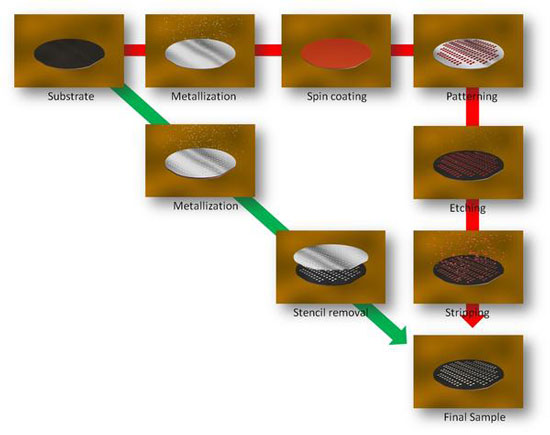
The principle of the "stencil" technique for making structures at the nanometer scale (a millionth of a millimeter) is simple: a substrate – a Silicon (Si) wafer or flexible plastics - is placed in an evaporator. On top of it stands a stencil with openings, called apertures, about 100-200 nanometers in size. During the metal evaporation, the stencil acts like a mask, and only the metal that passes through the apertures lands on the substrate. It is thus possible to locally deposit metal on the substrate in a very specific pattern. This precision is essential for the transistors or other electronic components made up of these structures to function properly.
"Take a piece of paper, cut a circle out of the middle. Put the rest of the paper against the wall, spray the whole thing with paint, and then remove the stencil. You have a nice circle. This is essentially the principle we're using," says Veronica Savu, who works in EPFL's Microsystems Laboratory, led by Professor Juergen Brugger. "Using stencils to make something isn't new, she continues. But to be able to do it at such a tiny scale is a real scientific challenge."
And Savu has already taken on the challenge. Her research was highlighted on the cover of the scientific journal Nanoscale this summer ("100 mm dynamic stencils pattern sub-micrometre structures"). She has also recently won a grant from the Swiss National Science Foundation to continue her work.
Movie illustrating dynamic stencil lithography: with the same aperture one can pattern custom geometries.
She is not satisfied with lithography that uses a static stencil, such as was described above, because it imposes several limitations; obtaining different patterns from a single stencil is impossible, for example. She's interested in dynamic stencil lithography (DSL), a novel process that enables custom designs using the same stencil.
"With a single aperture, our stencil can be moved during metal evaporation, and can draw several different two-dimensional patterns in a single operation, such as a square, a circle, a line or a cross. It's like writing a text with a pencil," she explains. "We have also proven that it is possible to use this method on a 100 mm-diameter substrate, the standard size used in industry." Up to this point, no one has managed to do everything that's needed to apply DSL at nanoscale in the real world. "We knew about DSL, about sub-micrometer size stencil openings, and about the use of stencils on industrial-size silicon samples. But nobody had yet been able to bring all those elements together in a single method."
Static or dynamic stencil lithography could thus eventually be used in industry, replacing the traditional so-called "resist-based" nanolithography methods. Those are complicated and expensive processes. "The use of stencils in the static mode represents a democratization of nanolithography – no need for expensive machinery, just a stencil and an evaporator," says Professor Brugger.
"Now, We are going to collaborate with the Nanoscience Center at the University of Basel to do tests that are needed to prove a real application of dynamic stencil lithography," Veronica Savu explains. "The goal is to eventually make functional transistors, possibly using graphene or nanowires, like we've already done with static stencil lithography."