| Posted: Jan 23, 2006 |
Successful development of an upright-type double-gate MOS transistor capable of ultra-large scale in(...) |
| (Nanowerk News) The National Institute for Advanced Industrial Science and Technology (AIST) and Tohoku University have succeeded in manufacturing a high-performance upright-type double gate MOS transistor capable of ultra-large scale integration using neutral beams which cannot damage silicon substrates. |
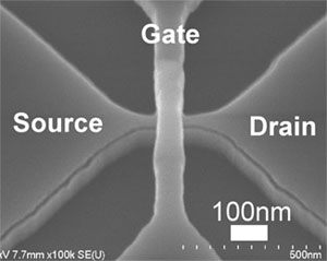 |
| An SEM image of an upright-type double-gate MOS transistor (Source: AIST) |
| In the semiconductor industry, global competition for developing and miniaturizing new materials has been increasing. Silicone plays a particularly important role for driving the semiconductor industry, so research and development of high performance silicone are very important for outpacing the competition. Successful development requires the miniaturization of high-performance integrated circuits. However, with conventional techniques designed for the fabrication of 2D-spreading devices, the amount of heat caused by leakage-current from the miniaturized circuit elements is so great that it is extremely difficult to develop ultra-large scale integration circuits for the 32-nm technology generation. |
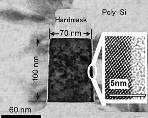 |
| A TEM image of the channel cross-section (Source: AIST) |
| To overcome such a technical barrier, AIST has been developing a 3D, upright-type double-gate MOS transistor, which not only can suppress the leakage-current that causes heat generation but can be highly integrated. Thus, combining this AIST technique with a nearly damage-free etching technique using neutral beams, which has been developed by Prof. Seiji Samukawa of Tohoku University, the researchers have created an upright-type double-gate MOS transistor which enables ultra-large scale integration. |
| This transistor has an etched surface flatness of less than 1 nm in irregularity, and has high electron mobility. Moreover, the performance of the transistor was found to be 30% better than that of the transistors fabricated by conventional processing techniques. This suggests that our technique may be promising for ultra-fine circuit fabrication in the 32-nm technology generation. |
| Source: AIST |

