| Oct 21, 2011 |
Imec uses Si nano-pillar test structures to evaluate advanced cleaning and drying techniques |
| (Nanowerk News) Imec in collaboration with Lam Research presents a new method for the quantitative evaluation of wafer drying techniques. The method uses Si nano-pillar test structures in combination with top-down scanning electron microscopy (TD-SEM) inspection. The use of Si nano-pillars with high aspect ratios (up to 28) brings new insights into the mechanisms of sticking and pattern collapse during wafer drying steps. These insights support the development of enhanced drying techniques that better preserve the stability of high-aspect-ratio nano-structures during wafer cleaning. |
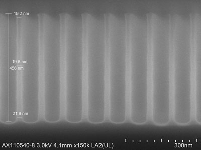 |
| Cross-section SEM image of Si nano-pillars after plasma etch and mask strip |
| As CMOS scaling continues, it becomes ever more challenging to preserve the stability of high-aspect-ratio nano-structures such as shallow trench isolators, gate structures and stacked capacitors. More specifically in wet cleaning processes, capillary forces exerted on nano-structures during wafer drying can lead to stiction or collapse of neighboring features. Therefore, the semiconductor community is eagerly looking for improved drying techniques that reduce the risk of stiction. However, the development of such techniques requires the availability of a dedicated test vehicle in combination with a quantitative metrology. Imec together with equipment supplier Lam Research now propose a novel test method that makes use of Si nano-pillar test structures and TD-SEM inspections. The method has been used to evaluate the effect of structure geometry, materials, and cleaning technique on pattern collapse, and to explore the potential of structure repair. |
| Nano-pillars were fabricated by first printing 90nm pitch nano-dots in 193nm photoresist. Subsequently, they were transferred into an amorphous carbon patterning layer and Si substrate using plasma etch technology on 300mm wafers. As such, Si nano-pillars were obtained with an aspect ratio up to 28. In contrast to other proposed test structures such as cantilevers and DRAM cylinders, these nano-pillars do not require any wet etch treatment during patterning, making the structures suitable for investigating various cleaning techniques. Inspection of collapse events after cleaning was performed using TD-SEM, followed by dedicated post-inspection image analysis. |
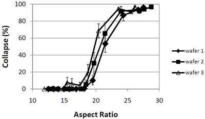 |
| Pattern collapse threshold curve for a specific cleaning–drying method. The percentage of collapse as a function of aspect ratio of the pillars at 90nm pitch is depicted. |
| A first observation is a sharp dependence of pattern collapse on aspect ratio. By measuring the percentage of collapse at different aspect ratios, a threshold aspect ratio can be defined below which the structures are stable. We investigated two cleaning methods and found threshold values of 18 and 13, respectively. Based on these results, we can conclude that the first method is superior to the second in terms of pattern collapse prevention. The experiments further suggest that the collapse events are at random and statistically determined within a pillar field. |
| Another important result is that once collapse occurred, repair is possible when applying HF chemistry, while de-ionized water rinses using a better drying technique do not restore the pattern. This finding proves that the deformation in pillar bending is elastic. Moreover it suggests a chemical bond formation between pillars under stiction similar as observed for particle ageing on silicon wafers. |
| More detailed results have been presented at the 220th Electrochemical Society (ECS) Meeting, October 2011. |
| Source: imec |

