| Nov 22, 2011 |
First proof of single atomic layer material with zero electrical resistance |
| (Nanowerk News) A research group at the NIMS International Center for Materials Nanoarchitectonics (MANA) proved that the electrical resistance of a metal single atomic layer on a silicon surface becomes zero by superconductivity. |
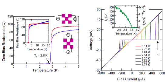 |
| (Left) Temperature dependence of zero bias resistance measured by attaching electrodes to a solid surface substance comprising an indium single atomic layer. The inset shows changes in a wider temperature region. Resistance becomes zero at a temperature of 2.8K. (Right) Bias current–voltage characteristics measured while changing temperature. When the bias current reaches the critical current value (Ic), superconductivity is destroyed and the substance switches to a state having normal resistance. The inset plots Ic and the critical current density (J3D,C) obtained from Ic, as functions of temperature. |
| A research group led by Dr. Takashi Uchihashi, a MANA Scientist, and Dr. Tomonobu Nakayama, a MANA Principal Investigator, both of the International Center for Materials Nanoarchitectonics, National Institute for Materials Science (President: Sukekatsu Ushioda), demonstrated that a substance comprising a metal single atomic layer on a silicon surface becomes free of electrical resistance by superconductivity. |
| The current mainstream integrated circuits using semiconductor devices generate excessive heat during operation, and this is a serious problem from the viewpoints of energy saving and environmental protection. Logic elements using superconductors have attracted attention as an effective candidate which offers a fundamental solution to this problem. On the other hand, research on quantum information communication using single photon detectors employing superconducting devices is also progressing as a means of communication which assures perfect information security. As issues for future practical application, it is necessary to realize high integration and high efficiency, etc. in these respective devices. Refinement and creation of thin films of superconducting materials are considered effective for this purpose. |
| Focusing on an indium single atomic layer arranged with a special structure on a silicon surface, the team led by Dr. Uchihashi observed for the first time in the world that the electrical resistance of this substance become zero, and the substance displays superconductivity, when cooled to a low temperature. Furthermore, when the current passing through this substance was increased, it was possible to pass a large current of 6.1√109 A/m2 (current density) at maximum. Based on the principle of superconductivity, it had been anticipated that a superconducting current (=current with zero resistance) would be difficult to pass through the extremely confined and disordered region at the surface of a solid. However, this research overturned that prospect. |
| This research clarified the fact that the thickness of superconducting materials can be reduced to the ultimate limit of the atomic level. It is considered that this achievement will accelerate research on further refinement/integration of superconducting logic elements and research on higher efficiency/higher speed in superconducting detectors. |
| These research results are scheduled for publication in the near future as an Editor's Suggestion in the journal of the American Institute of Physics, Physical Review Letters ("Macroscopic Superconducting Current through a Silicon Surface Reconstruction with Indium Adatoms"). |
| Source: NIMS |

