| Mar 15, 2012 |
Nano-imprinted photonic structures improve efficiency of silicon solar cells |
| (Nanowerk News) Imec has successfully fabricated crystalline silicon (c-Si) solar cells including 2D periodic photonic nanostructures made with nano-imprint lithography. The result was an improvement in energy-conversion efficiency, compared to unpatterned cells, through a better absorption of the light spectrum. The technique shows a path to further reducing the thickness of solar cells while keeping the efficiency as high as possible. |
| The reduction of the silicon wafer thickness from 150µm to 50µm and below is potentially the best way to decrease the cost of solar cells. At imec, we pursue this path through ultrathin-film crystalline silicon technologies. However, if thinner photoactive layers are used, the optical absorption is significantly reduced. This is especially so at the near-infrared region of the solar spectrum. A photon with a wavelength of 1µm needs an absorption depth as deep as 100µm. Losing this part of the spectrum reduces the overall conversion efficiency of the cells. |
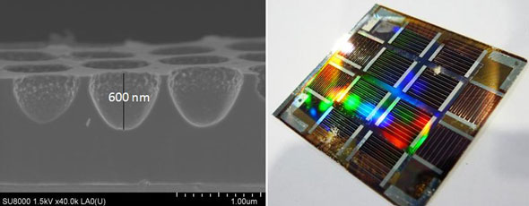 |
| (left) Cross section SEM of the 2D periodic photonic nanostructures, (right) 1-µm-thin crystalline silicon solar cells on glass including the 2D periodic photonic nanostructures with obvious diffraction of light. |
| Recently, the field of photonics has come up with methods to manipulate light through specific structures that are smaller than the wavelengths. This makes it possible to use periodic photonic nanostructures to affect the motion of photons in a similar way as the periodicity of atoms in a semiconductor crystal affects the motion of electrons. But to do so, we need efficient patterning techniques with nanometer-scale resolution. |
| At imec, we used nano-imprint lithography to fabricate 2D periodic photonic nanostructures. Nano-imprint lithography is a recent top-down approach for fabricating nanometer-scale patterns. It is one of the best candidates to improve the light absorption while maintaining an acceptable manufacturing cost, but it is currently barely used for c-Si PV applications. The patterning is performed by direct deformation of the resist material through mechanical pressure and a subsequent etching step. |
| Compared to the standard solar cell texturing by wet-etching, subwavelength patterning using nano-imprint lithography has some advantages. First, there is less material waste upon etching (less than a micron is consumed) compared to the state-of-the-art texturing, where 5-10 microns are lost. And second, diffraction and scattering of light is possible at higher angles due to the dimensions of the nanopattern. |
| Source: imec |

