| Mar 16, 2012 |
EU-funded BOOM project on SOI photonic integration technology successfully concluded |
| (Nanowerk News) Imec and its partners successfully completed 'BOOM', a EU-funded project coordinated by the National Technical University of Athens (NTUA). By systematically advancing silicon-on-insulator (SOI) photonic integration technology, compact, cost-effective and power efficient components have been developed that enable photonic Tb/s capacity systems for current and new generation high-speed broadband core networks. As part of the project, imec has realized an optical label extractor consisting of a high-resolution demultiplexer integrated with highly efficient photodetectors. |
| The European BOOM project has focused on the development of a photonic routing platform relying on hybrid SOI integrated photonic ICs to implement all the routing functionalities: label detection (imec), control signal generation (HHI, IHP), wavelength conversion (NTUA, TU/e, TU Berlin) and wavelength routing (Lionix, AMO). Finally, a routing machine with >160Gb/s aggregate capacity (NTUA, Telecom Italia Lab) was built. |
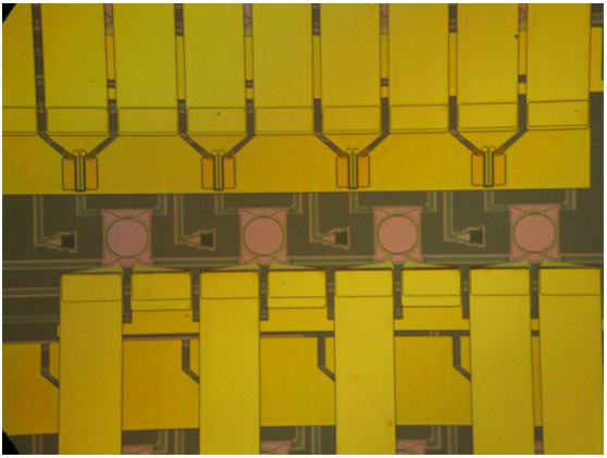 |
| Four channel label extractor with four high-finesse ring resonators integrated with InGaAs photodetectors. |
| This way, the project answered the growing demand for bandwidth hungry internet applications which stresses the available capacity and performance of current optical core networks. Power efficiency, physical size and equipment cost are key issues in these networks and increasingly more difficult to keep within acceptable limits. Electronic carrier routing systems consume and dissipate large amounts of electrical power and heat respectively. By bringing photonics technologies deeper and deeper within these routers their performance can be improved and power consumption can be decreased. |
| The imec work within the project focused on the optical label detector. In the proposed routing architecture the optical data packets are labeled with a wavelength code, which has to be extracted from the packet and sent to the routing unit. The label extractor consists of an optical demultiplexer with very high resolution – 12.5GHz – fabricated on the imec silicon photonics platform and integrated with high efficiency photodetectors. Reaching the required resolution turned out to be very challenging and required an in depth study of silicon microring resonators. The required specifications could be reached using single ring resonator based filters. The ring resonators have integrated resistors, which allow fine tuning of the wavelength channels (bottom electrodes) through the thermo-optic effect. They are connected to evanescently coupled InGaAs photodetectors using the heterogeneous integration technology developed by INTEC, imec's associated laboratory at Ghent University. The detectors had an efficiency of close to 1A/W and were operating at the specified speed of 1GBit/s (up to 5GBit/s). Finally the device was packaged in collaboration with Fraunhofer IZM group (Berlin). The device is now ready for operation in a system test bed. |
| The results obtained by imec in the project and in particular the exhaustive study on the microring resonators are not only relevant for realizing the optical label extractor. They also form an important input for the imec optical interconnect program which requires high performance demultiplexers for increasing the bandwidth in optical chip-to-chip links. Further they can be used in optical sensors and non-linear devices. |
| Source: imec |

