| Mar 16, 2012 |
New ways of shaping semiconductors |
| (Nanowerk News) Researchers from ETH Zurich and CSEM, in collaboration with their Italian colleagues from the Politecnico di Milano and Università di Milano-Bicocca, have developed a new method by which highly perfect structures composed of different semiconductors can be manufactured. First results are presented in the 16 March 2012 issue of Science ("Scaling Hetero-Epitaxy from Layers to Three-Dimensional Crystals"). |
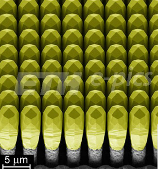 |
| Perspective scanning electron micrograph of an array of ~8 micrometers tall, facetted Germanium crystals grown on Silicon pillars (© ETH Zurich). |
| The novel structures can be manufactured to virtually any thicknesses on cheap and abundant silicon substrates. Instead of being assembled by state of the art bonding techniques, the structures are grown in one piece, i.e. monolithically, by deposition techniques customary in semiconductor processing. Thanks to this novel approach, crystal defects, normally present in layers of atoms differing in size, are entirely eliminated. Moreover, disruptive substrate bowing upon temperature changes, caused by unequal thermal expansion coefficients of dissimilar materials, is largely absent. Most importantly, fatal layer cracking induced by thermal stresses can no longer occur. |
| Resembling a chocolate bar |
| The basic idea leading to this remarkable behavior is very simple. Rather than consisting of continuous layers, the structures are composed of a space-filling array of individual crystals, separated by narrow gaps of several tens of nanometers. They are made in the following way. In a first step a silicon wafer is patterned by photolithography and subsequently etched into a structure resembling a chocolate bar. The depth of the trenches separating the elevated regions typically exceeds their width of a few micrometers. The desired three-dimensional semiconductor structures are then grown onto the substrate pillars under conditions assuring a minimum separation of neighboring crystals. The method has been perfected for defect-free germanium structures on top of silicon wafers, for which a record height of 50 µm was achieved. Based on the know-how gained in the course of this development, the research teams are confident that in the future the new concept will be transferrable to many other material combinations. |
| Novel applications in many fields |
| The ability to synthesize virtually defect-free monolithic semiconductor structures allows for novel applications in many fields. A particularly exciting example is given by energy-resolving X-ray imaging detectors with ultra-high spatial resolution. Here, thick germanium absorbers are ideally suited. They might result in far lower doses necessary for X-ray imaging in medical applications. High efficiency multiple-junction solar cells for concentrator and space applications are another example for which the new method offers substantial cost and weight reductions by replacing expensive, fragile and heavy germanium substrates by cheap and light silicon substrates of high mechanical stability. Another example of potential interest could be power electronic devices grown onto large silicon wafers. The Swiss groups participating in this research work are generously supported by the Nano-Tera project «NEXRAY» — Next Generation X-ray Systems - one goal of which is the development of novel X-ray imaging detectors. «CSEM is proud to coordinate such an interdisciplinary project involving CSEM, EMPA and ETH Zurich that will lead to new devices», stated Alex Dommann, Program Manager for MEMS at CSEM. |
| Source: ETH Zurich |

