| May 10, 2012 |
Nanotubes and silicon: unexpected ingredients in a new optical device
|
|
(Nanowerk News) "A lot of discoveries in the laboratory are purely accidental," said Swastik Kar, an assistant professor of physics in the College of Science.
|
|
He and Yung Joon Jung, an associate professor of mechanical and industrial engineering, have received a three-year, $309,000 National Science Foundation grant to explore a phenomenon they discovered entirely by chance, which could afford a new generation of extremely efficient electronics.
|
|
Kar's expertise is in the physics of graphene, which is a sheet of carbon atoms, one atom thick. Because of its structure, graphene is a superior thermal and electric conductor. Jung's work focuses on the mechanics of carbon nanotubes, or nanometer sized rolled-up sheets of graphene.
|
|
"The two materials are closely related in many ways," said Kar.
|
|
Last year, the Provost's office awarded Jung and Kar a Tier 1 Interdisciplinary Seed Grant to develop new optoelectronic and solar devices using both graphene and carbon nanotubes.
|
|
But their investigations weren't going as planned. Shining light on the devices generated a completely unexpected behavior.
|
|
"We kept getting a weird kind of response," said Kar. Added Jung: "We thought there must be something wrong."
|
|
So they decided to take a step back and remove the graphene from the equation, leaving a layer of carbon nanotubes over a silicon substrate. Lo and behold, Kar said, the results remained the same.
|
|
The weird responses had nothing to do with the graphene, but rather, were related to an unexpected property at the interface between the carbon nanotubes and the silicon.
|
|
Past research by other groups has shown that interactions between silicon atoms and carbon nanotubes can turn light into electrical current. "That is pretty much the basis of all photodiodes and solar cells," said Kar. "If such a device is held in darkness, there's little or no current at all. You shine light and current flows — it's called photocurrent."
|
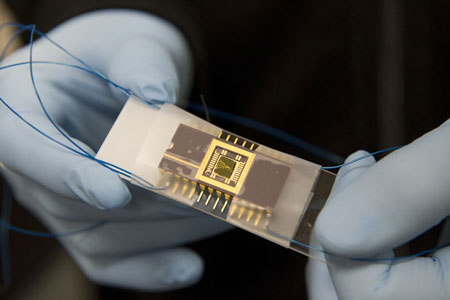 |
| One of the optoelectric devices made of silicon and carbon nanotubes.
|
|
But different from conventional diodes, the photocurrent in Kar and Jung's devices can be controlled by applying a voltage. "A few volts can change the photocurrent by up to four orders of magnitude. That is what makes it a very sensitive photoswitch," Kar said. "The photocurrent grows almost exponentially, resulting in large photocurrents for relatively small light intensities." They believe the behavior comes from the highly organized carbon nanotube architectures unique to Jung's lab.
|
|
Since only small amounts of light are required, the phenomenon could be useful for low power optoelectronics. A digital camera using the photoswitch, for example, could produce crisp images in very low light. If the behavior can work in the infrared spectrum, it could mean more efficient night-vision technologies.
|
|
But before it can be used in any practical application, the team must first understand the underlying physics of the phenomenon.
|
|
Kar's lab will quantify the behavior, mapping the physical properties of these curious devices while a collaborator in South Korea will use his expertise in theoretical physics to analyze the results computationally.
|
|
Ultimately, they hope the interdisciplinary approach will afford a better understanding of the behavior on an atomic level.
|
|
"That is the beauty of nanoscience and nanotechnology research," said Jung. "By collaborating with people from different backgrounds you can accomplish great things."
|

