| Posted: June 8, 2006 |
Successful development of a carbon nanotube transistor with over 1000 times operational stability |
| (Nanowerk News) The Institute of Scientific and Industrial Research, Osaka University, the >National Institute of Advanced Industrial Science and Technology (AIST), and Japan Science and Technology Agency have jointly succeeded in the development of a production process for a new carbon nanotube transistor (CNT transistor), and thereby succeeded in the development of a CNT transistor with an operational stability 1000 or more times that of conventional CNT transistors. |
| The gain of CNT transistors is 10-100 times that of the silicon transistors used for present day integrated circuits, and thus they hold promise as the next generation of transistors. |
| However, conventional CNT transistors have the disadvantage that their characteristics vary significantly with time and voltage, resulting in a big obstacle to practical use. |
| It has been considered that this transistor instability is caused by contamination due to water and oxygen adsorbed on the CNT surface. Osaka University and the AIST have jointly found that photoresist residues may also be one of the causes, and have succeeded in the development of a new production technique enabling the removal of the factors inducing the variation of the characteristics. Using this technique, the time variation of the characteristics can be reduced to within 0.01 %, and a hysteresis in the characteristics can be almost completely removed, realizing sufficient operational stability for practical use. |
| With this new technique, reliable CNT-transistors can be produced, enabling highly-sensitive biosensing and the detection of single biomolecules. |
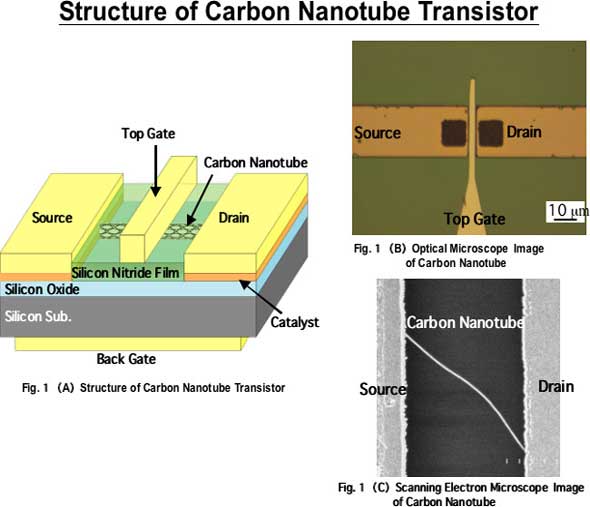 |
| Figure 1(A) shows a structural illustration of a CNT-FET produced, in which the CNTs are formed on a silicon oxide thin film/silicon substrate, and source- and drain-electrodes, made of metal, are formed on both ends of the CNT region to take out the electric current. Furthermore, it should be noticed that the surface of the CNTs are covered with a silicon nitride thin film. Furthermore, on the silicon nitride thin film, the top gate electrode, being capable of controlling the electric current flowing in the CNTs, is formed. On the rear side of the silicon substrate, the back gate, similarly controlling the electric current, is formed. Figure 1(B) shows an optical microscopic image of a CNT-FET we have developed. In this image, each metallic electrode is visible, while the CNTs are not visible, because they are formed under the gate electrode. Figure 1(C) shows a scanning electron microscopic image of a CNT between the electrodes. |
| Source: AIST |

