| Posted: June 3, 2008 |
IMEC and AIXTRON set important step towards low-cost GaN power devices |
| (Nanowerk News) IMEC, an independent European research center in the field of nanoelectronics, and AIXTRON, a metal-organic chemical-vapor deposition (MOCVD) equipment supplier, have demonstrated the growth of high-quality and uniform AlGaN/GaN heterostructures on 200mm silicon wafers. This demonstration is a milestone towards fabricating low-cost GaN power devices for high-efficiency/high-power systems beyond the silicon limits. |
| IMEC and AIXTRON deposited, for the first time ever, crack-free AlGaN/GaN structures onto 200mm Si(111) wafers. The layers show good crystalline quality as measured by high-resolution x-ray diffraction (HR-XRD). Excellent morphology and uniformity were obtained as well. The high-quality AlGaN and GaN layers were grown in AIXTRON’s application laboratory on the 300mm CRIUS metal-organic chemical-vapor-phase epitaxy (MOVPE) reactor. |
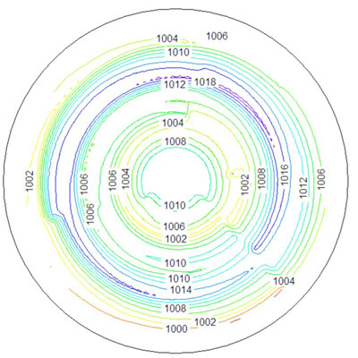 |
| Thickness uniformity map of a 1µm GaN layer deposited on 200mm Si(111) using an AlN/AlGaN buffer. The average thickness measured in-situ is 1008nm for the full wafer excluding a 5mm edge. (Image: IMEC) |
| “The demonstration of GaN growth on 200mm Si wafers is an important step towards processing GaN devices on large Si wafers”, said Marianne Germain, Program Manager of IMEC’s Efficient Power program. “There is a strong demand for GaN-based solid-state switching devices in the field of power conversion. However, bringing GaN devices to a level acceptable for most applications requires a drastic reduction in the cost of this technology. And that is only possible by processing on large-diameter Si wafers. 150mm, and then 200mm are the minimum wafer sizes we need to fully leverage today’s silicon processing capabilities.” The bow of the resulting wafers is still quite large, in the range of 100µm; but IMEC believes that an optimized buffer can reduce this bow drastically, enabling further processing. Marianne Germain: “We aim to further develop the growth process and to qualify the wafers to be compatible with Si-CMOS process.” |
| Gallium nitride (GaN) has outstanding capabilities for power, low-noise, high-frequency, high-temperature operations, even in harsh environment (radiation); it considerably extends the application field of solid-state devices. Due to the lack of commercially available GaN substrates, GaN heterostructures are nowadays grown mainly on sapphire and silicon carbide (SiC). Si is a very attractive alternative, being much cheaper than sapphire and SiC. Other benefits include the acceptable thermal conductivity of Si (half of that of SiC) and its availability in large quantities and large wafer sizes. But until now, Si wafers with (111) surface orientation were only available with a diameter up to 150mm. The 200mm wafers were custom-made by MEMC Electronic Materials, Inc. using the Czochralski growth (CZ) method. CZ wafers are ideally suited for switching applications with large breakdown voltages. For such devices, the performance is independent of the resistivity of the Si substrate. |
| Process details |
| For the AlGaN/GaN heterostructures, a standard layer stack, that had already been successfully demonstrated on 100 and 150mm Si(111) substrates, was used. |
| First an AlN layer was deposited onto the Si substrate, followed by an AlGaN buffer which provides compressive stress in the 1 micron thick GaN top layer. The stack was finished with a 20nm thin AlGaN (26% Al) layer and capped with a 2nm GaN layer. From in-situ measurements, researchers from IMEC were able to extract the thickness uniformity of the different layers which show a standard deviation well below 1% over the full 200mm wafers (5mm EE). |
| Source: IMEC |

