| Posted: January 19, 2009 |
Extremely flat fixtures for EUV exposure |
| (Nanowerk News) Exposing silicon wafers to light during chip manufacture requires special fixtures called chucks. Novel electrostatic chucks made of glass ceramics are incredibly flat. This prevents structural distortions on the exposure mask and the silicon chip. |
| Smaller, even smaller, tiny. Miniaturization in chip manufacture is progressing at an impressive pace. Researchers continue to push the physical limits of semiconductor technology and are developing methods of making circuit elements even smaller and faster. At the same time, the associated processes are having to meet increasingly high requirements. |
| The experts predict a promising future for EUV lithography – lithography with extremely shortwave ultraviolet light. This works as follows: Light with a wavelength of 13 nanometers is guided through a reflection mask onto the silicon wafers, where it generates nanometer structures. As the exposure processes take place in a vacuum, special fixtures are necessary to accommodate the silicon wafers and the exposure mask, and to hold them firmly in place. The technical term for these is chucks. |
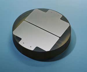 |
| Super-flat chuck |
| Researchers at the Fraunhofer Institute for Applied Optics and Precision Engineering IOF have developed exceptionally precise electrostatic chucks for EUV lithography. “The chucks need to be extremely smooth and even,” says Fraunhofer IOF scientist Dr. Gerhard Kalkowski. “If they are not super-flat, the result is height deviations in the mask, which lead to structural distortions on the silicon chips.” The IOF researchers are using special glass materials and have developed new technologies to increase the levelness of the chucks, with excellent results: While height deviations of over 100 nanometers had been measured previously, the new material reduced them to 74 nanometers, setting a new record. The chuck and the mask virtually merge into a single plane. The IOF chucks also have other advantages: “The material guarantees high holding strengths, distributed across the entire surface, and reduces abrasion,” says Kalkowski. Two properties of great importance to the EUV exposure process. |
| The researchers’ findings will greatly benefit the chip industry, as chip manufacturers rely particularly on the stability and precision of the chucks in order to be able to use EUV lithography in mass production. Meanwhile, the IOF researchers are working towards their next goal: flatter than 50 nanometers. |
| Source: Fraunhofer Gesellschaft |

