| Oct 13, 2017 |
Biodegradable electronics
|
|
(Nanowerk News) Under the direction of the Fraunhofer FEP, an in-house Fraunhofer project for development of biodegradable electronics was begun last year. The Fraunhofer Institutes ENAS, IBMT, ISC, and the Fraunhofer Project Group IWKS are working together on the project. First results of the Fraunhofer FEP will be presented during Semicon Europe 2017 as part of productronica 2017 in Munich at the Silicon-Saxony joint booth in Hall B, Booth No. B1-416, November 14-17, 2017.
|
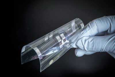 |
| Biodegradable conductor structures on biodegradable polymer film. (Image: Fraunhofer FEP)
|
|
Electronic devices that are completely broken down in a biological environment after a pre-defined operating life open up novel applications as well as ways for reducing their ecological footprint.
|
|
One enabling technology for such devices is the production of biodegradable conductive traces on biodegradable substrates using vacuum technologies. This technology was developed by Fraunhofer FEP.
|
|
A novel application area for these innovative electronic components for example is in the field of active medical implants that after expiration of their operating life are resorbed by tissue, thereby sparing the patient a second surgical intervention.
|
|
The Fraunhofer Gesellschaft e. V. is now funding the “bioElektron – Biodegradable Electronics for Active Implants" project through its in-house program (funding No. MAVO B31 301). The goal of the project is the development of essential components for biodegradable electronic parts that can be employed for example in an implant.
|
|
This includes in particular
|
|
biodegradable conductor structures
biodegradable electrodes for collecting electrical signals or delivering electrical stimulation
biodegradable thin-film transistors and circuitry
biodegradable barrier coatings as moisture and gas barriers, and electrical insulation layers
|
|
These elements will be monolithically integrated into a flexible thin-film device.
|
|
Conductor structures and organic thin-film transistors are being developed at Fraunhofer FEP using vacuum technology. Deposition of magnesium via thermal evaporation under high vacuum conditions is being used as an enabling technology for this purpose. Magnesium is known for being a biodegradable and biologically compatible metal that is already employed in clinical environments as an absorbable implant material.
|
|
The challenge consists of depositing this metal onto biodegradable polymer films that magnesium does not adhere sufficiently to under normal processing conditions. By suitably pre-treating the substrates using a combination of drying, plasma treatment, and utilization of seed layers, finely structured high-quality conductor structures have been produced.
|
|
“We are now prepared to discuss these results with interested partners from industry and the scientific community during productronica 2017 at the Silicon-Saxony joint booth (Hall B1, Booth B1-416) in order to be able to implement them in current practical applications”, explains Dr. Michael Hoffmann from Fraunhofer FEP and head of the bioElektron project.
|

