| Jun 20, 2012 |
First observation of plasmarons in graphene |
(Nanowerk News) An international team of scientists performing angle-resolved photoemission spectroscopy (ARPES) experiments at ALS Beamline 7.0.1 have found that composite particles called plasmarons play a vital role in determining graphene's properties (see paper in Science: "Observation of Plasmarons in Quasi-Freestanding Doped Graphene").
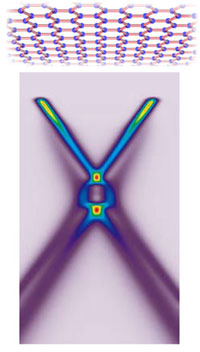 A theoretical model of plasmaron interactions in graphene, sheets of carbon one atom thick. A plasmaron consists of a charge carrier (electron or hole) coupled with a plasmon—an electron density wave. Although plasmarons were proposed theoretically in the late 1960s, and indirect evidence of them has been found, this work is the first observation of their distinct energy bands in graphene, or indeed in any material. The discovery may hasten the day when graphene can be used for "plasmonics" to build ultrafast computers—perhaps even room-temperature quantum computers—plus a wide range of other tools and applications. On the usual band-gap diagram of neutral graphene, the filled valence band and the empty conduction band are shown as two cones that meet at their tips at a point called the Dirac crossing. This picture of graphene's simple conical bands is not a complete description, however; instead it's an idealized picture of "bare" electrons. Even in initial ARPES experiments with graphene, the researchers suspected that the situation was not quite as simple as the two-cone, bare-electron model suggested. At low resolution, there appeared to be a kink in the bands at the Dirac crossing. Because there really is no such thing as a bare electron, the researchers wondered if this fuzziness was caused by charge carriers emitting plasmons. Because theorists thought that there should be an even stronger effect, the researchers wondered if the graphene's silicon-carbide substrate was influencing the physics. A single layer of carbon atoms resting on a silicon-carbide substrate isn't the same as free-standing graphene. The substrate could in principle weaken the interactions between charges in the graphene (on most substrates the electronic properties of graphene are disturbed, and the plasmonic effects can't be observed). Therefore the team introduced hydrogen atoms that bonded to the underlying silicon carbide, isolating the graphene layer from the substrate and reducing its influence. Now the graphene film was flat enough to study with ARPES but sufficiently isolated to reveal its intrinsic interactions.> |
| The images obtained by ARPES actually reflect the dynamics of the holes left behind after photoemission of the electrons. The lifetime and mass of excited holes are strongly subject to scattering from other excitations such as phonons (vibrations of the atoms in the crystal lattice) or by creating new electron–hole pairs. In the case of graphene, the electron can leave behind either an ordinary hole or a hole bound to a plasmon—a plasmaron. |
| Taken together, the interactions dramatically influenced the ARPES spectrum. When the researchers deposited potassium atoms atop the layer of carbon atoms to add extra electrons to the graphene, a detailed ARPES picture of the Dirac crossing region emerged. It revealed that the energy bands of graphene cross at three places, not one. Ordinary holes have two conical bands that meet at a single point, just as in the bare-electron, noninteracting picture. But another pair of conical bands, the plasmaron bands, meets at a second, lower Dirac crossing. Between these crossings lies a ring where the hole and plasmaron bands cross. |
| Plasmons can be excited by photons from external sources. Photonics is the field that includes the control and use of light for information processing; plasmons can be directed through channels measured on the nanoscale (billionths of a meter), much smaller than in conventional photonic devices. And since the density of graphene's electric charge carriers can easily be influenced, it is straightforward to tune the electronic properties of graphene nanostructures. For these and other reasons, graphene is a promising candidate for much smaller, much faster devices—nanoscale plasmonic devices that merge electronics and photonics. |
| Source: Berkeley Lab |

