| Dec 21, 2012 |
'Carbon Galaxy' and other amazing nanotechnology images
|
|
(Nanowerk News) Here is another installment of our collection of amazing images from nanotechnology labs from all over the world. You can find other nanotechnology images here.
|
|
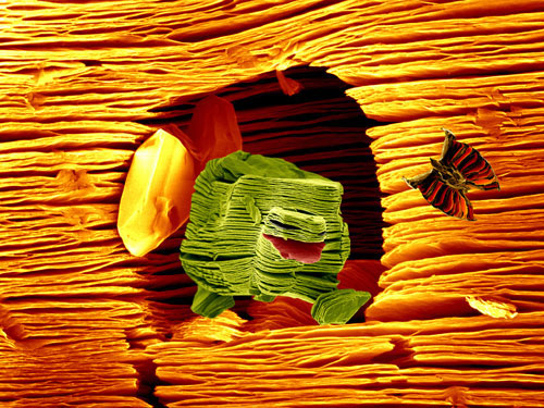
Visualization methods provide an important tool in materials science for the analysis and presentation of scientific work. Images can often convey information in a way that tables of data or equations cannot match. Occasionally, scientific images transcend their role as a medium for transmitting information, and contain the aesthetic qualities that transform them into objects of beauty and art.
|
|
As a special feature of recent MRS Meetings, the MRS has offered the popular Science as Art competitions, with entry open to all registered meeting attendees. The images below represent the winners of the 2012 MRS Fall Meeting Science as Art competition.
|
|
You can see all galleries here on the MRS website: Science as Art
|
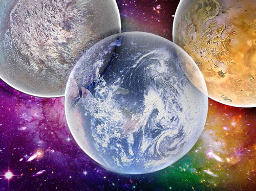 |
| Carbon Galaxy. Scanning electron micrograph of spherical carbon particles, prepared at high temperature and pressure, mimics the galaxy. Technologically, these spherical particles are of interest as lithium-ion battery electrodes and as lubrication additives to reduce friction and wear in gasoline-powered engines. (Vilas Pol, Michael Tackeray, Dean Miller and Michele Nelson, Argonne National Laboratory) ©MRS
|
|
|
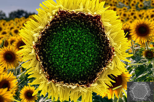 |
| Not your average sunflower. Colorized SEM image of ZnO crystallites blooming on the surface of single crystalline hexage of gold. The gold plate is obtained through solution-based thermolysis. The ZnO is nucleated and grown through a 2-step solution synthesis. (John Joo, Harvard University; Background image of sunflowers was taken by Monica Scanlan) ©MRS
|
|
|
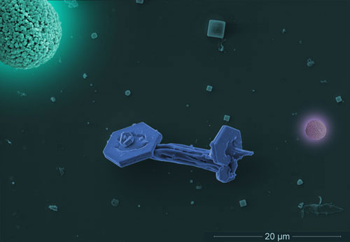 |
| Micro Spacecraft. The collage shows two false color SEM images. The ZnS spacecraft (~20 µm in length) predominantly consists of hexagonal platelets, which are obtained by thermal decomposition of a molecular source under solvothermal conditions. The globular planets represent porous LiFePO4 microspheres (~3 µm in diameter) prepared by a solvothermal approach. (Sven Barth, Vienna University of Technology) ©MRS
|
|
|
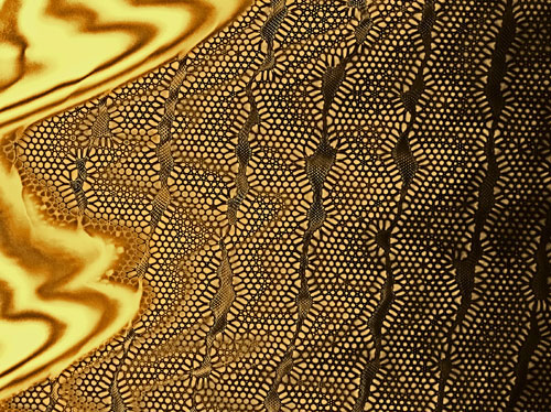 |
| Screw dislocation network in alumina. Screw dislocation network formed in a (0001) / [0001] twist grain boundary in an alumina bicrystal. The network consists of hexagonal units due to the three-fold symmetry about the c-axis, and the size of each unit is about 50nm. The ribbon-like structures lying along the vertical direction correspond to planar voids between the crystals. The image was taken along the [0001] zone axis by using a transmission electron microscope (JEOL, JEM-2010HC, 200kV). (Eita Tochigi, University of Tokyo) ©MRS
|
|
|
 |
| The Happy 2D World. 2-D Ti3C2 layers were produced by etching Al from Ti3AIC2, a member of the ternary transition metal carbides called MAX Phases. Given its similarities with graphene, it was labeled MXene." (Babak Anasori, Michael Naguib, Yury Gogotsi and Michel W. Barsoum, Drexel University) ©MRS
|
|
We have a collection of these amazing images in some of our articles on Nanowerk. You can find the links here.
|

