| Jan 31, 2013 |
The fastest clock rate in the universe
|
|
(Nanowerk News) Switches are omnipresent in computers as they are crucial to manipulate information encoded as bits. To greatly improve the speed with which information is processed, much work is being done worldwide to realize optical switches that control information encoded as light pulses. Scientists from the University of Twente in the Netherlands, and the Institute for Nanoscience and Cryogenics (CEA/INAC) in France have managed to repeatedly and reproducibly switch-on and switch-off an optical cavity at a world-record clock rate of 1.4 THz, or 350 times faster than an electronic switch operates at 4 GHz. Switching at THz clock rate is achieved by avoiding absorption that leads to world record level minimum energy loss per switch event.
|
|
The results will be published in the leading American journal Optics Letters ("All-optical switching of a microcavity repeated at terahertz rates"), and are expected to yield ultrafast optical data communication, and perhaps even switches for quantum bits of information.
|
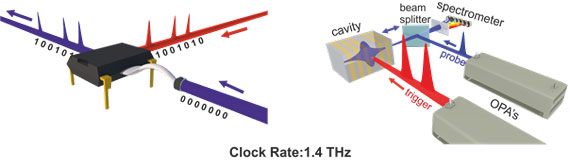 |
| Figure 1: Cartoon of how the ultrafast all-optical modulator works. (Left panel): The beam shown in blue, is used to transmit data, enters the modulator carrying no information at first (right port). The information carried by the red beam, responsible for switching, is encoded on the blue beam and transferred (left port). In this way information can be transferred from one color to another. (Right panel): Schematic of the experimental setup. The probe beam (at telecom frequency) is shown in blue and trigger beam in red. Similar to left panel, by switching the cavity with the trigger pulse we can modulate the probe light, which is stored in the cavity.
|
|
Cavities are widely used in optics for their ability to store light in a small volume for a particular duration in time. In the cavity light bounces back and forth between the mirrors. Since light is an electromagnetic wave, it appears that only waves whose wavelength (or color) matches the cavity length can exist in the cavity. This is the result of constructive interference where crests and valleys of many waves coincide, and therefore add up to a high intensity. As a result, the allowed waves resonate to form a standing wave in the cavity, as shown in Figure 1.
|
|
Light does not circulate indefinitely inside a cavity, since on every roundtrip a little bit of light leaks out. The light waves that escape from the cavity are selectively transmitted, giving the opportunity to select the color of light to work with. All other colors of light are reflected from the front of the cavity.
|
|
In modern science and technology, cavities fabricated from semiconductor materials such as GaAs and AlAs have become highly popular. The reason is that these cavities can be made very small with lengths of the order of microns, that is, only 1/100th of the thickness of a human hair. Therefore these microcavities can be integrated on chips, and are used in modern appliances such as miniature lasers to read or write data in a DVD player. Semiconductor microcavities are also employed to transmit email, internet, and tv-messages as optical signals.
|
|
To route or steer information in optical pulses, it is essential to have light-steering devices whose properties can be changed in time, that is: switched. To date, the properties of a microcavity were switched by electrical current in the semiconductor materials. These processes are limited by for instance how fast electric charges flow away, and which are relatively slow. Consequently, the speed of such switches does not take full advantage of the unrivalled speed of light.
|
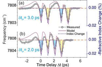 |
| Figure 2: Measured (circles) and theoretical (red curve) resonance frequency of the cavity versus time delay between signal and trigger pulses. The resonance frequency quickly decreases before returning to the unswitched value. The switch-on and off cycle takes less than 1ps. The model matches the experimental observations well.
|
|
The method realized by the Dutch-French team works as follows. They shine a signal pulse on a semiconductor microcavity that was made by precise nanofabrication techniques. They measure the cavities? resonance wavelength, see Figure 2. The scientists also shine a trigger laser pulse that instantaneously changes the properties of the microcavity by using the so-called electronic Kerr effect. The hurdle that the team overcame was to tune the color of the trigger laser to long wavelengths in order to avoid absorption of light. They managed to avoid absorption which also leads to world record level minimum energy loss per switch event. They took advantage of the extremely fast motion of electrons in semiconductor that literally dance to the beat of the laser light. As a result, the properties of the cavity are only switched when both the signal and the trigger pulses are present.
|
|
Figure 2 shows that during the switching process, the cavity resonance quickly becomes lower and returns to its starting situation. It appears that the speed of the switch is determined by how fast the signal light escapes from the microcavity. The switch-on and -off occur within one picosecond, or one millionth of a millionth second. The switching of the cavity is repeated reproducibly at THz clock rates for the first time. This fantastic repetition rate may best be conceived of by realizing that within that time light travels about 1/100th of a centimeter.
|
|
The new switch is versatile since it is not restricted to a particular kind of semiconductor material or cavity design. Even more exciting is that the switch is repeated every picosecond at a record level of energy loss. In other words, information is steered at a rate in excess of 1000 THz, which is about 350 times faster than the clock speed of a fast personal computer. Therefore, the new switch brings within reach on-chip beyond-terahertz switching rates for data communication. Since computer speed is currently being raised by parallel processing, the proposed switch method implies a quantum leap in process speed.
|
|
The team
|
|
The research has been performed by M.Sc. Emre Y?ce, Dr. Georgios Ctistis, Robin D. Buijs, Bob de Ronde, Prof. Dr. Allard P. Mosk, and Prof. Dr. Willem L. Vos from the Complex Photonic Systems (COPS) Chair at the MESA+ Institute for Nanotechnology of the University of Twente in Enschede, The Netherlands, in close collaboration with Dr. Julien Claudon, Dr. Emmanuel Dupuy, and Prof. Dr. Jean-Michel G?rard from the Institute for Nanoscience and Cryogeny (CEA/INAC) in Grenoble, France.
|

