| Feb 06, 2013 |
Researchers report dual approach to achieving record TFET device performance |
| (Nanowerk News) Researchers at the University of Notre Dame have produced tunnel field effect transistors (TFETs) with record-high drive current. The results were presented on December 12 at the International Electron Devices Meeting (IEDM 2012) in San Francisco [G. Zhou et al, IEDM 2012, session 32.6]. |
| Complementary metal oxide semiconductor (CMOS) transistors are the building blocks of silicon-based digital, analog, and mixed-signal electronics. However, CMOS technology is approaching fundamental limits that prohibit further miniaturization. TFETs can deliver subthreshold swing lower than the thermal limit (60 mV/decade at room temperature) and thus operate at a supply voltage lower than today's CMOS technology. |
| "TFETs have the potential to significantly lower power consumption in future generation electronics, however, a major issue is their relatively low on-currents," says Huili Grace Xing, O'Hara Professor of Electrical Engineering. "In TFETs, electrons need to 'tunnel' through energy barriers to deliver current, which is a normal behavior at the quantum level, but the tunneling probability is usually low, which in turn limits the on-current." |
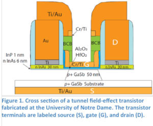 |
| The reported approach in realizing TFETs with record performance builds on previous work at Notre Dame, where the team created a new vertical structure. The new findings reported at IEDM show how to improve the TFET on-current in two ways. First, the team adopted a heterojunction based on indium arsenide (InAs) and gallium antimonide (GaSb). This heterojunction in the bulk form has a broken-gap energy band alignment, a very special band alignment that allows electrons to flow freely between the conduction band of InAs and the valence band of GaSb. |
| TFET device cross section imageHowever, in a thin slab of InAs electrostatically controlled by a gate on top (see device cross section), the energy band alignment to the underlying GaSb can be tuned by the gate voltage to be staggered (low tunneling probability) or broken-gap (high tunneling probability), thus enabling more efficient control of tunneling and enable high on-current. |
| Second, a novel device structure and process flow was designed to minimize the effects of parasitic resistances, thus improving the device characteristics. |
| The demonstrated record performance in tunnel FETs improved understanding of the device physics, which should portend more advances in the coming years. |
| Source: University of Notre Dame |

