| Jul 09, 2013 |
New method allows damage free cryogenic etching of ultralow-k dielectrics |
| (Nanowerk News) Imec today announced a cryogenic etching method that protects the surface of porous ultralow-k dielectrics against excessive plasma induced damages. |
| As semiconductor technology scales below the 20nm node, the capacitance increases between nearby conductive portions of high-density integrated circuits, resulting in loss of speed and cross-talk of the device. To control the increase in capacitance in deeply-scaled devices, insulating layers of porous low-k dielectrics are integrated through plasma etching. However, plasma etching exposes the dielectrics to active plasma radicals that penetrate deeply into the porous substrate, which then react and change the composition of the dielectric. |
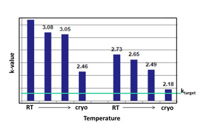 |
| Etching at cryogenic temperature results in targeted k-value. |
| To bypass such damages, imec developed a new cryogenic etching method. By applying very low (cryogenic) temperatures during etching, a condensation of etch products in the pores of the low-k material, results in a protection of the dielectrics’ surface. Imec demonstrated the method on a porous organosilicate (OSG) film. The results showed that no carbon depletion occurred when the wafer temperature remained below a certain critical level during plasma etching |
| “Our cryogenic etch method solves a key issue to further advancing scaling limits. It overcomes the disadvantages of current methods used to reduce plasma induced damage, such as dielectric etch at regular temperatures or low-k repair or high temperature pore stuffing, and it enables sub k=2.0 materials for integration,” stated Zsolt Tokei, program director interconnect at imec. “Our method is a true solution to further drive the development of next-generation, deeply-scaled technologies.” |
| Imec exhibits at SEMICON West, July 9-11, 2013. To learn more about imec and its new cryogenic etching method, please visit booth 1741, South hall. |
| Source: imec |

