| Oct 02, 2013 |
New biomimetic material to develop nanosensors
|
|
(Nanowerk News) The new features of this biomimetic material will allow researchers to develop multiple nanometer-sized chemical sensors over the same substrate by electron beam lithography, as a result, multifunctional biochips of major versatility will be developed. The possibility to record at nanometric scale is an essential benefit facing traditional biomimetic materials since this new material developed by researchers at the Universidad Politécnica de Madrid (UPM) and the Universidad Complutense (UCM) within the framework of Moncloa campus provides commercial potential applications.
|
|
This material is compound by a cross-linking linear polymer whose molecular structure is altered by the bombing with electrons. In this way, it is possible to use an electron beam of a few nanometers thick, as if it were an ultra fine point pencil, to write a pattern over a movie of this material adhered to a substrate. After the writing (lithography), the movie is submerged in a liquid developer able to dissolve the film area irradiated by the beam and to leave intact the non irradiated pattern over the substrate.
|
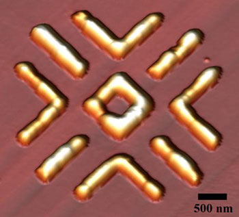 |
| This pattern represents the logo of Moncloa Campus, a topographic image taken with an atomic force microscope of biomimetic polymeric material developed by electron beam lithography. (Image: UPM)
|
|
In addition, the material behaves as a molecularly imprinted polymer (MIP), that is, it is able to recognize a molecule or a specific compound after a printing process at molecular level. The MIPs are synthetic materials with similar functionality to certain biological molecules, such as antigens and antibodies, used as receptors to detect certain molecules, for that reason MIPs are considered as biomimetic materials. The main benefits of the MIPs over the biological receptors are higher resistance to chemicals and extreme weather, lower cost and the ability to create synthetic chemical receptors inexistent in nature.
|
|
To date, in order to develop sensors, the methods used to record films in MIPs are based on printing and photolithography techniques. The main drawback of the printing method is the possible contamination of film surfaces of MIP which are in contact with printing molds, whereas the photolithography technique is not suitable to create nanometrics reasons. The new material can be recorded at nanometric scale with no need of mold of mask.
|
|
Researchers at the UPM and the UCM have developed nanometrics patterns of this material over silicon substrates by using an electron beam and proving the functionality of the MIP. The material is able to recognize the Rhodamine 123, which is a fluorescent molecule of high sensitivity and selectivity over other rhodamines. The methodology used to develop this material can be applied to the synthesis of other materials susceptible to be recorded by beam of electrons and able to detect substance of interest in toxicology and biomedicine.
|
|
The development of nanometrics structures of sensor materials has a double purpose. Firstly, a higher interaction between the sensor and the environment where the analyte is detected, increasing the speed and sensitivity detection. Secondly, the slight size of the sensor structures allow us to integrate multiple elements in just one chip o substrate saving costs and increasing its reliability and functionality of trials.
|
|
The method of development of this material was protected by a patent
|
|
This project was funded by the former Ministry of Science and Innovation within the framework of Explora project whose main researcher was Carlos Angulo Barrios of the Institute of Optoelectronics Systems and Microtechnology (ISOM) of the UPM. The EXPLORA projects are oriented to promote scientific curiosity, searching for creative research proposals resulting in a deep reflection on a given problem.
|

