| Oct 11, 2013 |
Nanoimprinting technique makes it possible to fabricate visible-light-bending metamaterials at unprecedented scales |
| (Nanowerk News) Artificial materials containing arrays of metal nanostructures can interact with light in useful and interesting ways. One of the most interesting possible uses of such ‘metamaterials’ is to bend light around objects, rendering them invisible. However, metamaterials usually only interact with light over a very narrow range of wavelengths—typically long wavelengths far beyond those visible to the human eye. |
| Takuo Tanaka from the RIKEN Metamaterials Laboratory, in collaboration with Shoichi Kubo and colleagues at Tohoku University, has now demonstrated a scalable fabrication method that greatly eases the production of metamaterials that can interact with light at visible wavelengths ("Split-ring resonators interacting with a magnetic field at visible frequencies"). |
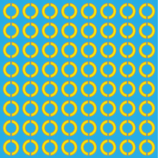 |
| Figure 1: Illustration of an array of gold split-ring resonators in a silica substrate. (Image: Takuo Tanaka, RIKEN Metamaterials Laboratory) |
| Tanaka and his team created a silica-based metamaterial containing an array of split-ring resonators—thin gold rings with two small breaks at the top and bottom (Fig. 1). A similar design previously proved successful when used at longer wavelengths in the microwave region. In principle, modifying the structure to function at visible wavelengths only requires the resonators to be made smaller to match the shorter wavelengths of visible light. However, the features required for such visible-light metamaterials are below 100 nanometers in size. Metamaterials are commonly fabricated by electron-beam lithography, which involves using a beam of electrons to draw out each resonator one at a time. This process is painstakingly slow, particularly for the production of the millions of small features needed to create a visible-light metamaterial of a practical size. |
| Instead, the researchers fabricated their structures through a process known as nanoimprint lithography. This technique involves transferring a master mold of the desired design onto a thin polymer film and then using standard metallization techniques to recreate the pattern in gold. In this way, the team was able to create split rings approximately 212 nanometers across and 54 nanometers high. |
| Tanaka and his colleagues demonstrated that their metamaterial magnetically interacts with red light. More important, however, is the scalability of their fabrication technique. Whereas techniques such as electron-beam lithography are limited to producing arrays of just several hundred square micrometers in area, Tanaka and his co-workers managed to create an array of 360 million split-ring resonators across a 5-millimeter square using their nanoimprint technique. “This is, to the best of our knowledge, the world’s largest two-dimensional split-ring resonator array metamaterial for visible light,” explains Tanaka. “Our next step will be to create much larger metamaterials, to make them three dimensional, and to reduce the operation wavelength.” |
| Source: RIKEN |

