| Oct 21, 2013 |
Grant funds development of improved nanoscale additive manufacturing (3D printing)
|
|
(Nanowerk News) A new Department of Energy grant will fund research to advance an additive manufacturing technique for fabricating three-dimensional (3D) nanoscale structures from a variety of materials. Using high-speed, thermally-energized jets to deliver both precursor materials and inert gas, the research will focus on dramatically accelerating growth, improving the purity and increasing the aspect ratio of the 3D structures.
|
|
Known as focused electron beam induced deposition (FEBID), the technique delivers a tightly-focused beam of high energy electrons and an energetic jet of thermally excited precursor gases – both confined to the same spot on a substrate. Secondary electrons generated when the electron beam strikes the substrate cause decomposition of the precursor molecules, forming nanoscale 3D structures whose size, shape and location can be precisely controlled. This gas-jet assisted FEBID technique allows fabrication of high-purity nanoscale structures using a wide range of materials and combination of materials.
|
|
By allowing the rapid atom-by-atom “direct writing” of materials with controlled shape and topology, the work could lead to a nanoscale version of the 3D printing processes now revolutionizing fabrication of structures at the macro scale. The technique could be used to produce nano-electromechanical sensors and actuators, to modify the morphology and composition of nanstructured optical and magnetic materials to yield unique properties, and to engineer high performance interconnect interfaces for graphene and carbon nanotube-based electronic devices.
|
|
"This unique nanofabrication approach opens up new opportunities for on-demand growth of structures with high aspect ratios made from high-purity materials," said Andrei Fedorov, the project’s leader and a professor in the Woodruff School of Mechanical Engineering at the Georgia Institute of Technology. "By providing truly nanoscale control of geometries, it will impact a broad range of applications in nanoelectronics and biosensing."
|
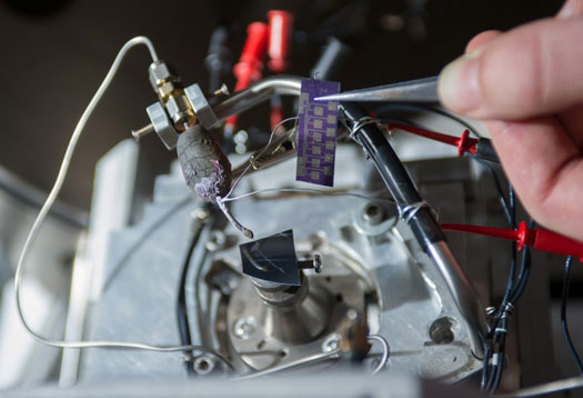 |
| This image shows a heated capillary micro-nozzle installed on the deposition stage of an FEBID system, along with the test chip used for electrical characterization of deposits for graphene interconnects.
|
|
Researchers have demonstrated the feasibility of the technique, and expect the three-year $660,000 grant to help them develop a fundamental understanding of how the process works, accelerate the rate of materials growth and provide improved control over the process. The research will include both theoretical modeling and experimental evaluation. Proof of principle for using thermally-energized gas jets as part of the FEBID technique was reported by Fedorov’s group in the journal Applied Physics Letters in 2011.
|
|
"Wherever electrons strike the surface, you can grow the deposit," explained Fedorov. "That provides a tool for growing complex three-dimensional structures from a variety of materials with resolution at the tens of nanometers. Electron beam induced deposition is much like inkjet printing, except that it uses electrons and precursor molecules in a vacuum chamber."
|
|
Two major challenges lie ahead for using the technique to manufacture 3D nanostructures: increasing the rate of deposition and eliminating the unwanted deposits of carbon that are formed as part of the process. To address these challenges, Fedorov and his team are using energetic jets of inert argon gas to clean substrate surfaces and carefully tune the energy of the desired molecules delivered in another jet to enhance the rate at which the precursor sticks to the substrate.
|
|
"If the energy of the jet is sufficiently high, the inert gas molecules striking the surface can knock away the adsorbed hydrocarbon contamination so that there is no parasitic carbon co-deposition," he said. "We can also tune the properties of the precursor molecules so they stick more effectively to the surface. We have shown that we can increase the rate of growth by an order of magnitude or more while maintaining a high aspect ratio of deposited nanostructures."
|
|
Overall, about two dozen materials have been successfully deposited using FEBID on different substrates, including semiconductors, dielectrics, metals and even plastics. The researchers also plan to create nanostructures containing more than one material, allowing them to create unique properties not available in each individual material. Examples might include new types of ferromagnetic materials and photonic bandgap structures with unique properties.
|
|
Fedorov’s group has used FEBID to fabricate low-resistance contacts to carbon nanotubes and graphene, a unique carbon-based material with attractive electronic properties.
|
|
Major technical challenges for the project include making tightly focused jets of thermally-energized precursor molecules to provide precise control of the fabrication. In operation, precursor molecules enter the reaction chamber from the micron-scale nozzle at sonic speeds, and accelerate in the vacuum environment to even greater speed, forming a molecular beam that impinges on the substrate. To make structures of the desired morphology, researchers will have to control the spreading of the generated molecular beam and its energy state at the point of contract with the substrate.
|
|
"We will be growing structures ranging in size from tens to hundreds of nanometers," Fedorov noted. "This means we will not only have to confine electrons to very small regions, but we will also need to confine the precursor molecules to these same domains."
|
|
The FEBID technique will likely not be used for high-volume fabrication because the process is difficult to scale up, Fedorov said. Accelerating the deposition rate will allow more rapid fabrication, but the 3D structures will still need to be produced one at a time. A partial solution to the scale-up challenge lies in the use of multiple electron beams and precursor jets operating in parallel.
|
|
The new technique will allow researchers to take better advantage of the unique properties of materials at the nanometer scale. Researchers will also have to account for those differences in developing the new manufacturing technique, as the interactions between electrons, precursor materials in the jet and substrate continually change with growth of the deposit.
|
|
"This research will open up the potential for some new discoveries in areas we may not be able to predict now," said Fedorov. "We need to understand the basic physics of what is happening. That basic understanding could lead us to some truly unique applied capabilities, and the possibilities are almost limitless."
|

