| Nov 14, 2013 |
Penn State launches new center to study atomic layer materials
|
|
(Nanowerk News) The promise of nanoscale science is that useful and unprecedented properties appear when materials are shrunk to the size of 100 nanometers or less. Now, Penn State and the Materials Research Institute have launched a center to discover what new properties can be created when atom-thick 2-dimensional layers of elemental materials and chemical compounds are formed or when those layers are built up into completely new 3-dimensional structures.
|
|
Mauricio Terrones, the center’s director and a professor of physics, chemistry and materials science and engineering at Penn State, announced the creation of the Penn State Center for Two-Dimensional and Layered Materials to an audience of more than 70 academic, government, and industrial scientists at a workshop earlier this year. At that meeting, Terrones reminded the scientists of nanotechnology’s foundational text, the talk by Nobel physicist Richard Feynman titled “There is Plenty of Room at the Bottom” at Caltech in 1959, which pointed to the possibility of building new materials from atom-thick layers of materials and of the new phenomena that could arise from doing so. What was a science fiction daydream in 1959 is an accomplished fact today.
|
 |
| CAPTION
|
|
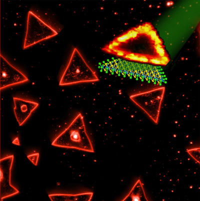
Two-dimensional systems based on the carbon atom have caused considerable excitement in the scientific community over the past two decades. The isolation of graphene, a single atom-thick layer of carbon, can be considered a defining point in the research and development of stable two-dimensional (2D) materials from layered systems. In fact, the fundamental studies on graphene resulted in the Nobel Prize in Physics (2010) in near record time. Additionally, discovery of graphene derivatives has also led to the Nobel Prize in Chemistry (fullerenes, 1996), and two Kavli Prizes in Nanoscience (nanotubes, 2008 and 2012).
|
|
Beyond graphene
|
|
However, graphene is only the tip of the iceberg. There is a whole market basketful of synthetic materials that can be isolated into 2D systems, with properties ranging from insulating and semiconducting to metallic and superconducting. Chemical compound materials such as boron nitride (h-BN), Molybdenum disulfide (MoS2), and Tungsten disulfide (WS2) exhibit novel properties at the atomic scale that could be exploited in new types of devices. For example, atom-thick h-BN, which is an insulator (ca. 5.6 eV), constitutes the thinnest insulator ever realized and may be the key for ultra-scaled semiconductor devices. On the other hand, transition metal dichalcogenides (TMDs), such as MoS2 and WS2, exhibit tunable electronic properties, which could be used in the realization of advanced optoelectronic devices, catalysis, transistors, sensors, valley polarization devices, spintronic components, lubricants, components in medical devices for diagnosis and treatment, etc. In the future, these 2D layered materials could be mixed to form completely new hybrid 3D layered structures with a wide range of applications not yet imagined.
|
|
Other possible applications for 2D and layered materials are in battery electrodes, flexible electronics, large area displays, and new transistors that can shrink features down to the 1nm scale.
|
|
Center expands
|
|
A dozen Penn State faculty members are involved in the center, including theorists, materials chemists, experimental physicists, experts in 2D synthesis, electron microscopists, super-fast-optics engineers, and device fabrication researchers. In addition, other research groups from Rice University, Florida State, and Southern Illinois University are also members. A second Beyond Graphene workshop is planned for Spring 2014.
|
|
For more information about the center, contact Mauricio Terrones at [email protected], or associate director, Joshua Robinson at [email protected].
|

